Why Substrate Choice Matters
Nanoscale Secondary Ion Mass Spectrometry (NanoSIMS) offers unparalleled spatial resolution (down to 50 nm) for isotopic and trace element analysis. However, the quality of your data is directly tied to the quality of your sample preparation.
Unlike standard microscopy, NanoSIMS relies on the extraction of secondary ions from the sample surface via a strong electric field. Therefore, the physical properties of the substrate—specifically conductivity, flatness, and vacuum compatibility—are critical for maintaining focus and preventing charging artifacts.
Get Your 4 Inch Silicon Wafer Quote FAST!

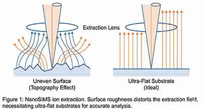
Figure 1: The NanoSIMS ion extraction process. Surface topography can distort the extraction field, highlighting the need for ultra-flat substrates.
Critical Substrate Specifications
1. Surface Topography (Flatness)
Topography is the enemy of NanoSIMS resolution. The instrument uses a high-voltage extraction field to pull ions into the mass spectrometer.
2. Electrical Conductivity
Because the sample is bombarded with charged particles (Cs+ or O-), non-conductive surfaces will accumulate charge. This "charging" deflects the primary beam and ruins the analysis.
- Conductive Substrates: Doped Silicon wafers, gold foil, or conductive metals are preferred.
- Non-Conductive Samples: Must be coated with a thin layer (5-30 nm) of Gold (Au), Gold-Palladium (Au-Pd), or Carbon (C) prior to analysis.
3. Vacuum Compatibility
NanoSIMS operates under Ultra-High Vacuum (UHV) conditions (approx 10-10 Torr). Substrates must not outgas.
- Avoid: Standard porous ceramics, volatile glues, or standard biological mounting media.
- Use: Vacuum-compatible epoxies (e.g., Araldite, Körapox), Indium mounts, or clean metal surfaces.
Standard Dimensions & Holders
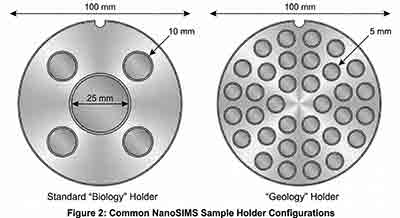
NanoSIMS instruments generally use specific multi-sample holders. Your substrate must fit physically within these strict tolerances.
| Parameter | Specification | Notes |
|---|---|---|
| Diameter | 5 mm, 10 mm, 12.7 mm (1/2"), or 25.4 mm (1") | Most common holders accept 10mm rounds ("bullets") or 1-inch rounds. |
| Thickness | Max 4-5 mm | Thinner is better. Standard Si wafers (500 µm) are ideal. |
| Edge Clearance | ~0.5 mm outer rim | The holder lip covers the outer edge; place samples centrally. |

Figure 2: Common NanoSIMS sample holder configurations (Standard "Biology" holder vs "Geology" holder).
Commonly Used Substrate Types
Depending on your application (Biology, Geology, or Material Science), choose one of the following:
Silicon Wafers (Doped)
The gold standard for biological sections and thin films. They are atomically flat and conductive (if Boron/Phosphorus doped). Usually cut into 5x5mm or 10x10mm chips.
Pressed Indium Mounts
Ideal for geological grains (Zircons, etc.). Grains are pressed into soft, high-purity Indium to ensure conductivity and flatness without using epoxy.
TEM Grids
NanoSIMS can analyze TEM grids, but they must be mounted on a solid, flat support (like a Cu or Si disk) to prevent grid deformation and ensure good heat dissipation.
Final Preparation Checklist
- Sample fits within 10mm or 25mm diameter circle.
- Thickness is less than 5mm.
- Surface is mirror-polished (roughness < 1µm).
- Sample is conductive or has been sputter-coated.
- Sample is dry and free of volatiles (vacuum safe).
- Region of Interest (ROI) is mapped (e.g., SEM or Fluorescence map provided).
