Consult with Our Optical Materials Experts
Need guidance choosing the right LiNbO₃ wafer?
Our engineers can help match your requirements for polish, doping, and thickness to your
optical or quantum device design.
Get Your Quote FAST! Or, Buy Online and Start Researching Today!
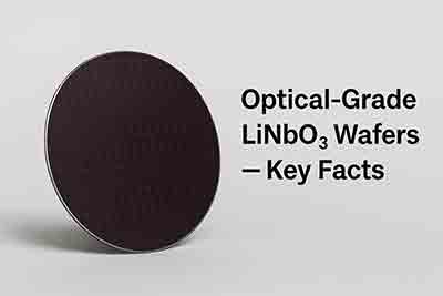
Optical-Grade LiNbO₃ Wafers — Key Facts
Lithium Niobate (LiNbO₃) is a cornerstone material in photonics, known for combining
high optical transparency, electro-optic activity, and
mechanical stability in one crystal.
Core Facts
- Transparency range: ≈350 nm – 5200 nm (visible to IR).
- Refractive index: n ≈ 2.2–2.3, ideal for tight light confinement.
- Electro-optic coefficient: r33 ≈ 30 pm/V — enables fast optical modulation.
- Curie temperature: ≈1140 °C — excellent thermal stability.
Optical-Grade Standards
- Defined by surface polish, crystal perfection, and low birefringence error.
- Used for high-precision EO modulators, waveguides, and frequency converters.
- Absence of twinning and sub-nanometer roughness ensures clear transmission.
Why Orientation Matters
- Z-cut: Maximizes EO effect for modulators.
- X-cut: Balanced optical/acoustic coupling.
- Y-cut & 128°Y-X: Best for SAW and RF applications.
Doping & Variants
- MgO-doped: Resists optical damage in high-power use.
- Fe-doped: Used for photorefractive storage and holography.
- PPLN: Enables quasi-phase matching for SHG, OPO, and DFG.
Practical Advantages
- Low optical loss and high modulation depth in telecom systems.
- Compatible with hybrid platforms (Si, SiN, or LNOI).
- Long lifespan and radiation resistance for aerospace and sensing.
Quick Takeaway
Choosing the right optical-grade LiNbO₃ wafer means balancing orientation,
doping, polish, and thickness to meet the optical, mechanical, and environmental
requirements of your device.
1. Understanding Crystal Orientation
Optical-grade Lithium Niobate wafers are manufactured in several orientations, each providing
unique advantages for optical, acoustic, or electro-optic devices. X-cut wafers
are oriented perpendicular to the X-axis, offering excellent electro-optic properties and strong
piezoelectric coupling—ideal for modulators and switches where light propagates along the Z-axis.
Y-cut wafers are valued for balanced acoustic and optical behavior and are commonly
used in acoustic-optic devices. Z-cut wafers yield the highest electro-optic coefficient
(r33 ≈ 30 pm/V) and are the industry standard for frequency conversion and high-speed
modulators. Orientation directly determines how electric fields interact with light, influencing
modulation depth, insertion loss, and drive voltage.

2. Surface Quality and Polish
Surface finish is one of the most critical parameters defining whether a LiNbO₃ wafer can be
classified as optical grade. Surface irregularities scatter light, reduce transmission, and degrade
signal quality in modulators or interferometers. Double-side-polished (DSP) wafers are recommended
for transmission optics because they minimize scattering and enable uniform propagation through the
crystal. Single-side-polished (SSP) wafers may be chosen for reflective or cost-sensitive designs where
only one surface interacts optically.
Surface roughness (Ra) below 0.5 nm is standard for high-performance optics, while
ultra-smooth surfaces approaching 1–2 Å are required for UV or high-power systems.
Scratch-dig specifications, following MIL-PRF-13830B standards, typically range from 20-10
for precision work to 10-5 for demanding interferometric or quantum photonic setups.
Each metric directly influences transmission efficiency and wavefront distortion.
3. Dimensions and Thickness
Selecting the correct wafer diameter and thickness ensures compatibility with optical benches,
deposition tools, and bonding equipment. Typical diameters include 2-inch (50.8 mm)
wafers for laboratory research and 3-inch (76.2 mm) wafers for small-scale production.
Thicker wafers offer mechanical stability but may introduce higher drive voltages in modulators, while
thinner wafers improve electrical efficiency at the cost of rigidity. Standard thicknesses range from
0.2 mm to 3 mm, with flatness control better than λ/10 at 633 nm and bow/warp below
30 µm for optical precision.
4. Doping and Advanced Variants
Doping alters the internal charge distribution and enhances optical performance.
MgO-doped LiNbO₃ (≈ 5–7 mol %) is used to suppress photorefractive damage,
particularly for high-power or temperature-variable environments.
Fe-doping improves photorefractive recording sensitivity in holography and data
storage, while PPLN (Periodically Poled LiNbO₃) introduces domain inversion for
quasi-phase-matched nonlinear processes such as SHG and OPO.
LNOI (Thin-Film LiNbO₃ on Insulator) combines high refractive-index contrast with
compact photonic integration for next-generation modulators and frequency converters.
5. Quality Control and Testing
Ensuring true optical-grade quality requires multiple inspection stages.
X-ray diffraction (XRD) confirms crystal orientation,
atomic force microscopy (AFM) measures nanometer-level surface roughness, and
interferometric profiling checks flatness and total thickness variation.
Optical inspection verifies the absence of twinning and domain boundaries that can scatter or distort
light. High-end wafers show dislocation densities below 10²–10³ cm⁻² and minimal strain, guaranteeing
consistent optical phase propagation across the entire substrate.
6. Application-Specific Insights
For electro-optic modulators, Z-cut wafers (0.5–1 mm thick, Ra < 0.5 nm)
provide optimal overlap between electric field and optical mode, reducing required drive voltage.
Frequency-conversion devices use Z-cut or periodically poled substrates to exploit
the d₃₃ coefficient for maximal SHG or DFG efficiency.
Surface acoustic-wave (SAW) filters benefit from 128°Y-X cuts with high coupling
coefficients and stable temperature performance. Each application depends on balancing cut, thickness,
and polish to achieve desired optical and mechanical outcomes.
7. Educational Summary
Choosing an optical-grade LiNbO₃ wafer is not just a purchasing decision but a
design choice that defines device performance. Understanding how surface polish,
orientation, doping, and thickness interact helps engineers tailor wafers for applications
ranging from telecommunications to quantum light generation. The insights provided here
form the foundation for developing high-efficiency, low-loss optical components that meet
the stringent standards of modern photonics research and industry.

