
A photovoltaic researcher requested customized patterned ITO on PEN for flexible OPV device fabrication. The requested ITO sheet resistance ranged from a few ohms per square up to approximately 30 Ω/sq, with a quantity of approximately 25–30 pieces.
ITO & Flexible Substrates for Organic Photovoltaic Research
UniversityWafer supplies substrates for organic photovoltaic (OPV) and organic solar cell (OSC) research, including rigid and flexible substrates suitable for thin-film device fabrication. Researchers can request indium tin oxide (ITO) coated substrates with specifications tailored to experimental device requirements.
ITO is widely used as a transparent conductive electrode in photovoltaic and optoelectronic devices because it combines relatively high electrical conductivity with good optical transmission across much of the visible spectrum. In many conventional OPV architectures, an ITO-coated substrate serves as one of the transparent electrodes through which light enters the device.
Patterned ITO on Flexible PEN Substrates
Flexible organic photovoltaic devices can be fabricated on polymer substrates such as polyethylene naphthalate (PEN). Compared with rigid glass, PEN enables lightweight and mechanically flexible device structures, making it useful for research involving flexible electronics, wearable devices, conformable photovoltaics, and other thin-film applications.
UniversityWafer can help researchers source custom patterned ITO substrates for experimental OPV fabrication. Important specifications may include substrate material, dimensions, ITO thickness, sheet resistance, optical transmission, surface properties, pattern geometry, and quantity.
Example Research Request
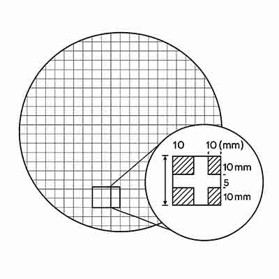
Reference #325282 for example specifications and pricing.
Why Substrate Selection Matters in OPV Devices
The substrate is more than a mechanical support for an organic solar cell. Its optical, electrical, thermal, and surface properties can affect device fabrication and performance. For transparent-electrode architectures, the substrate/electrode combination must provide sufficient optical transmission while maintaining suitable electrical conductivity.
Researchers designing flexible OPV devices should also consider surface roughness, dimensional stability, thermal processing limits, electrode adhesion, sheet resistance, and mechanical flexibility. These factors can influence coating uniformity, interface quality, series resistance, device yield, and long-term stability.
Common OPV Substrate Considerations
- Transparent electrode: ITO is commonly used where a transparent conductive contact is required.
- Sheet resistance: Lower electrode resistance can help reduce resistive losses, although conductivity must be balanced with transparency and process requirements.
- Optical transmission: The substrate and transparent electrode should transmit the wavelengths needed by the photoactive layer.
- Surface quality: A clean, sufficiently smooth surface supports uniform deposition of thin organic and interfacial layers.
- Thermal compatibility: Flexible polymer substrates generally impose lower processing-temperature limits than glass or semiconductor wafers.
- Mechanical flexibility: PEN and related polymer films can support bendable and lightweight photovoltaic device designs.
- Patterning: Custom electrode geometries can define active device areas and electrical contacts for experimental OPV structures.
Request Custom OPV Research Substrates
Tell us the substrate material, dimensions, ITO sheet resistance, ITO pattern, thickness requirements, surface specifications, and quantity needed for your experiment. We can help identify substrate options for organic photovoltaic and flexible thin-film research.
Get Your OPV Substrate Quote FAST! Or, Buy Wafers Online and Start Your Research Today!
How Do Organic Solar Cells Work?
Organic solar cells (OSCs), also known as organic photovoltaics (OPVs), convert light into electrical energy using semiconducting organic materials. Unlike crystalline silicon solar cells, OPVs commonly use a thin photoactive layer containing electron-donor and electron-acceptor materials.
Many modern OPVs use a bulk heterojunction (BHJ), in which donor and acceptor materials form nanoscale interpenetrating domains. This architecture creates a large donor-acceptor interfacial area that assists exciton dissociation and subsequent charge generation.
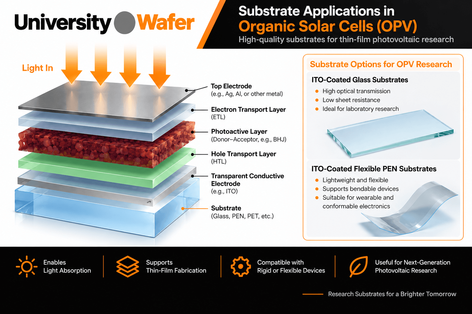
Organic Solar Cell Working Principle
1. Light Absorption and Exciton Generation
When the photoactive organic semiconductor absorbs a photon with sufficient energy, an electron is promoted to an excited state. Because organic semiconductors generally have relatively low dielectric constants, the photoexcited electron and hole initially remain Coulombically associated, forming a bound excited state called an exciton.
2. Exciton Diffusion
The exciton must reach a suitable donor-acceptor interface before it recombines. Exciton diffusion lengths in many organic semiconductors are relatively short, which is one reason nanoscale control of the donor-acceptor morphology is important in high-performance OPV devices.
In a bulk heterojunction, the donor and acceptor phases are intermixed on the nanoscale, increasing the probability that a photogenerated exciton reaches an interface where charge transfer can occur.
3. Interfacial Charge Transfer and Separation
At the donor-acceptor interface, favorable energy-level alignment can drive electron transfer from the excited donor toward the acceptor, producing an interfacial charge-transfer state. The electron and hole must then separate sufficiently to form mobile charge carriers rather than recombine.
Efficient charge generation therefore depends not only on donor and acceptor energy levels, but also on molecular packing, interfacial energetics, morphology, dielectric properties, and competing recombination processes.
4. Charge Transport and Collection
After charge separation, electrons and holes move through their respective transport pathways toward opposite electrodes. Electrons generally travel through the electron-accepting phase, while holes travel through the electron-donating phase.
Interfacial layers between the active layer and electrodes are often used to improve charge selectivity, reduce recombination, and optimize energy-level alignment. A transparent conducting electrode such as indium tin oxide (ITO) is commonly used on the light-entry side of many OPV device architectures.
Typical Organic Solar Cell Structure
The exact layer sequence depends on whether the device uses a conventional or inverted architecture, but a research OPV may contain:
- Substrate: glass, PEN, PET, or another suitable rigid or flexible material
- Transparent electrode: commonly ITO or another transparent conductive material
- Charge-selective layer: assists electron or hole extraction
- Photoactive layer: donor-acceptor organic semiconductor system
- Opposite charge-selective layer: improves carrier selectivity and extraction
- Top electrode: selected according to the device architecture
- Encapsulation: protects sensitive layers from oxygen, moisture, and other environmental exposure
Materials Used in Organic Photovoltaics
OPV research has investigated many combinations of conjugated polymers, small molecules, fullerene derivatives, and non-fullerene acceptors (NFAs). The optimum combination depends on absorption spectrum, energy-level alignment, charge transport, film morphology, processing conditions, and device architecture.
Examples of Donor Materials
- P3HT
- PTB7 and related polymers
- PM6
- PBDB-T family materials
Examples of Acceptor Materials
- Fullerene derivatives such as PCBM
- Non-fullerene acceptors such as Y-series materials
Material systems continue to evolve rapidly, so researchers should select donor-acceptor combinations based on the requirements of the specific experiment rather than assuming one material pair is optimal for every OPV.
Organic Solar Cells vs. Silicon Solar Cells
| Characteristic | Organic Solar Cells | Crystalline Silicon Solar Cells |
|---|---|---|
| Semiconductor | Organic molecules or conjugated polymers | Crystalline silicon |
| Initial Photoexcitation | Typically produces strongly bound excitons | Readily produces mobile electron-hole carriers under operating conditions |
| Charge Generation | Often relies on donor-acceptor interfaces | Carrier separation is supported by device junctions and selective contacts |
| Active Semiconductor Thickness | Typically sub-micrometer thin films | Typically much thicker than OPV active layers |
| Substrate Options | Can be fabricated on rigid or flexible substrates | Conventional cells use rigid crystalline silicon wafers |
| Processing | Many materials are compatible with solution coating and printing | Established wafer-based semiconductor manufacturing |
| Mechanical Flexibility | Flexible devices are possible with suitable substrates and electrodes | Conventional crystalline silicon wafers are relatively rigid and brittle |
| Technology Maturity | Active research and emerging commercial applications | Mature, large-scale commercial technology |
Advantages of Organic Photovoltaics
OPV technology is attractive because organic semiconductor layers can be extremely thin and may be compatible with lightweight, flexible, and large-area substrates.
- Lightweight: very thin active and transport layers can reduce device mass.
- Flexible: compatible device stacks can be fabricated on polymer films such as PEN.
- Solution processing: many organic semiconductor systems can be deposited from solution.
- Large-area manufacturing potential: coating and printing methods may enable scalable production.
- Optical tunability: molecular design can modify absorption and electronic properties.
- Semi-transparent devices: certain architectures can be engineered for partial visible-light transmission.
Challenges in Organic Solar Cell Research
OPVs also present significant engineering challenges. Device performance depends strongly on material selection, morphology, interfaces, electrodes, substrate properties, and environmental stability.
- Operational stability: organic materials and interfaces can degrade under prolonged illumination, heat, oxygen, or moisture exposure.
- Encapsulation: effective barrier layers may be necessary to protect environmentally sensitive device components.
- Morphology control: nanoscale donor-acceptor morphology strongly affects exciton harvesting, charge transport, and recombination.
- Scaling: performance achieved on small laboratory cells does not automatically translate to large-area modules.
- Electrode resistance: transparent electrode sheet resistance becomes increasingly important as device area increases.
- Interface engineering: contact materials and interfacial layers can significantly influence voltage, fill factor, charge extraction, and stability.
What Determines OPV Efficiency?
Organic solar cell performance is commonly characterized by power conversion efficiency (PCE), which depends primarily on the device's open-circuit voltage (VOC), short-circuit current density (JSC), and fill factor (FF), relative to the incident optical power.
OPV efficiency can be affected by:
- absorption of the solar spectrum
- exciton generation and diffusion
- charge-transfer and separation efficiency
- donor-acceptor morphology
- electron and hole transport
- recombination losses
- electrode and contact resistance
- active-layer thickness and uniformity
- optical interference within the device stack
- device area and fabrication quality
How Much Do Organic Solar Cells Cost?
There is no single representative price for an organic solar cell. Costs vary considerably between laboratory-scale devices, prototype modules, research materials, and commercial products.
For research applications, cost depends on factors such as the substrate, transparent conductive coating, electrode patterning, organic semiconductor materials, deposition process, device area, encapsulation, and quantity. For this reason, experimental OPV substrate requirements are generally better evaluated from the required specifications rather than a generic price per cell or price per watt.
OPV Substrates for Flexible & Thin-Film Research
Substrate selection can affect optical transmission, electrode conductivity, surface quality, processing temperature, mechanical behavior, and ultimately device fabrication. Researchers developing flexible OPVs may use ITO-coated PEN or other transparent substrates, while rigid laboratory devices are frequently fabricated on transparent conductive glass.
UniversityWafer can help researchers source substrate materials for organic photovoltaics, flexible electronics, thin-film devices, transparent electrodes, and related optoelectronic research.
Related Organic Photovoltaic & Thin-Film Research
Explore related substrate materials, conductive coatings, and fabrication technologies used in photovoltaic and optoelectronic research.
- Indium Tin Oxide (ITO) Substrates – Transparent conductive ITO-coated substrates for photovoltaic, display, sensor, and optoelectronic research.
- FTO Substrates – Fluorine-doped tin oxide conductive substrates for solar cell and thin-film device research.
- Photodiode Research – Substrate materials and information for light-detection and optoelectronic device research.
- Thin-Film Deposition – Learn about thin-film deposition processes used to form functional layers on research substrates.
- Solar Cell Substrates – Explore substrate materials for photovoltaic and next-generation solar cell research.
- Glass Wafers & Substrates – Glass substrate options for optical, photovoltaic, MEMS, and thin-film device fabrication.