
Need Help Preparing Your Mask Data?
Our engineers can assist with layer separation, biasing, tone inversion, OPC, and data verification for all major formats (GDSII, OASIS, DXF, Gerber). Ensure your pattern is fully production-ready before fabrication.
Get Your Quote FAST! Or, Buy Online and Start Researching Today!
Available Mask Sizes
- 5″ × 5″: standard IC/MEMS masks
- 6″ × 6″ and 7″ × 7″: stepper reticles and projection systems
- 9″ × 9″: large-area exposure and panel lithography
Material Options
- Soda-lime glass: cost-effective for contact lithography
- Quartz: low CTE and UV transparency for DUV steppers
- Emulsion/Mylar: economical for PCB and microfluidic use
Supported File Formats
- GDSII and OASIS (preferred)
- DXF and Gerber (for PCB layouts)
- Bitmap and image conversions available on request
Turnaround Options
- Standard: 5–7 business days
- Rush: 48–72 hours
- Super-Rush: 24 hours (depending on complexity)
Data Prep Services
- Layer separation and design verification (DRC)
- Optical Proximity Correction (OPC) and biasing
- Tone inversion (dark/clear field)
- Fracturing and fractal fill for e-beam writing
Pellicle & Inspection Options
- Pellicles for i-line, DUV, and EUV exposure bands
- Automated CD/overlay inspection
- Metrology reports and defect maps available
Handling & Storage
- Store in cleanroom or anti-static containers
- Handle by edges; avoid touching the chrome surface
- Keep pellicle-mounted masks in low-humidity environments
Photomasks Overview
UniversityWafer provides custom chrome-on-glass and quartz photomasks for research and manufacturing applications including IC, MEMS, sensors, photonics, and biomedical devices. Masks are written directly from GDSII, OASIS, DXF, or Gerber data using precision laser and electron-beam (e-beam) writers. We support single-layer to multi-level designs, from rapid prototype work to full wafer-production reticles.
Mask Substrates & Materials
Our photomasks are fabricated on soda-lime glass, fused silica (quartz), or film (Mylar/emulsion) substrates. Chrome (Cr) films typically range from 80 nm – 120 nm with optional CrOx anti-reflective coating for reduced standing-wave effects and improved optical contrast. Quartz masks are recommended for DUV (248 nm / 193 nm) lithography, while soda-lime is ideal for i-line (365 nm) contact/proximity exposure tools.
Applications in Research & Development
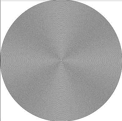
UniversityWafer masks are used in advanced research labs worldwide, including biomedical, microfluidic, MEMS, and semiconductor research. One highlighted case is a cancer-research project where a client required a chrome-on-glass photomask with concentric circle patterns used for tissue culture and optical measurement alignment. The patterned area measured 19 mm × 19 mm, featuring 25 µm line widths and 50 µm periods. This mask, produced for cancer-detection studies, was fabricated with a 120 nm chrome layer and delivered within five business days with standard visual inspection and checkplot verification.
Writing Technologies & Capabilities
- Laser writing: 1 µm minimum feature, fast turn-around (ideal for MEMS, PCB, and fluidic chips).
- E-beam writing: 0.25 µm critical dimension (CD) capability with excellent overlay control.
- Data prep: includes fracturing, biasing, tone inversion, OPC (optical proximity correction), and DRC verification.
- Formats supported: GDSII • OASIS • DXF • Gerber • Bitmap conversions upon request.
All designs are checked for feature integrity and tone consistency before exposure. Customers receive checkplots for approval prior to fabrication.
Mask Types
- Binary Chrome Masks: dark-field or clear-field, used in contact/proximity and stepper lithography.
- Stepper Reticles (4× / 5×): quartz masks for IC and advanced MEMS production.
- Gray-tone / Half-tone Masks: variable-transmission masks for 3D resist shaping, microlenses, and grayscale lithography.
- Emulsion / Mylar Masks: cost-effective options for PCB, microfluidic, and rapid prototype use.
Optical Tone & Polarity
Tone defines whether the exposed region corresponds to the transparent or opaque area: dark-field masks show transparent device features with a chrome background, while clear-field masks show opaque device features on a clear background. Our data team can perform tone inversion or layer separation automatically when files are submitted.
Precision & Tolerances
- Minimum feature size: 0.25 µm (e-beam) | 1 µm (laser) | ≥ 5 µm (film).
- CD tolerance: ± 0.1 µm (e-beam) | ± 0.3 µm (laser).
- Overlay accuracy: ≤ 0.25 µm (1σ) for reticles | ≤ 1 µm for contact masks.
- Surface flatness: ≤ 1 µm bow typical for 7″ quartz substrates.
Pellicles & Inspection
Pellicles are available for i-line, DUV, and EUV applications to prevent contamination-induced print defects. Each mask undergoes optical and automated inspection under cleanroom conditions. CD and defect metrology reports can be supplied upon request. Optional pellicle mounting ensures mask longevity and cleanliness during high-volume lithography.
Common Specifications
- Mask sizes: 5″ × 5″, 6″ × 6″, 7″ × 7″, 9″ × 9″
- Film thickness: 80–120 nm Cr, optional CrOx anti-reflective layer
- Wavelengths: 365 nm (i-line), 248 nm, 193 nm (DUV)
- Turnaround: Standard 5–7 days • Rush 48–72 hrs • Super-rush 24 hrs (layout-dependent)
Ordering Guidelines
- Specify mask size, substrate (glass, quartz, or film), and tone (dark/clear field).
- Provide minimum feature size, CD/overlay target, and wavelength.
- Attach design files in GDSII, OASIS, DXF, or Gerber format with layer labels.
- Indicate pellicle requirements, quantity, and inspection level.
- Optional: request CD/overlay reports or gray-tone calibration for optical depth control.