
We are using the silicon wafers as conducting substrate for cross sectional scanning electron microscopy. The specs would be conductive and polished surface on one side.
Silicon Wafers Used for SEM
Researchers have used the following test grade silicon wafers for their Scanning Electron Microscopy studies.
Researcher:
Si Item #452 (Buy online and save!)
100mm P(100) 0-100 ohm-cm SSP 500um
Get Your Quote FAST! Or, Order Online and Start Researching Today!
Ultra-Pure Silicon for SEM
A Ph.D. asked the following question:
Question:
Can I use this wafer (undoped silicon wafer) to drop my samples for Scanning Electron Microscopy?
Answer:
Ultra-Pure Silicon wafer Item #2313 are made with Oxygen content<1ppma, Carbon content<1ppma and all electronically active dopants and impurities < 0.001ppma.
Reference #221060 for specs and pricing.
Can undoped silicon wafers used for Scanning Electron Microscopy?
Undoped silicon wafers can be used for Scanning Electron Microscopy (SEM). Silicon wafers are commonly used as substrates for sample preparation in SEM. The key reason for using silicon wafers is their excellent mechanical stability, thermal conductivity, and flat, uniform surfaces, essential for high-resolution imaging.
Undoped silicon wafers have a very low concentration of impurities, which means they have a high purity level and helps to minimize the background signal in the SEM images, making it easier to observe the sample features and obtain accurate, high-quality images.
When using silicon wafers for SEM, the samples are generally mounted on the wafer using various techniques, such as drop-casting, spin-coating, or sputter-coating. Once the sample is attached to the wafer, it can be inserted into the SEM for imaging.
It is important to remember that the type of silicon wafer, its surface treatment, and the sample mounting method can all affect the quality of SEM images. Therefore, it is crucial to choose the appropriate wafer and mounting technique based on the specific requirements of a researcher experiments.
Silicon Wafers Used for Polymer Analysis
A researcher from a large university requested the following:
We would require 10 silicon wafers to be used for polymer analysis, preferably silicon wafers compatible with piranha treatment. The analytes would be 100-300nm nanoplastic particles to be dripped in a dry-ice flash freezing method from standards onto the wafer surface. The SEM to be used is an Apreo Variable Pressure SEM, your advice on the correct wafer would be appreciated.
Reference 268006 for pricing.
Tips For Polymer Analysis
Polymer characterization is the analytical branch of polymer science. Its goal is to identify the properties of polymers that have a specific function in the environment. As polymers undergo different processes, they exhibit various properties that make them useful in various fields. Here are some tips for determining the properties of different polymers. Using a suitable method, you can ensure the quality of your products. Polymer characterization should be carried out by professionals in the field.
Optimisation of separation methods is an important component of any successful polymer characterization process. A good separation technique helps identify the structure of the polymer by determining its molecular weight. This method is fast and versatile and is applicable to both synthesis and quality control. Moreover, you can determine the structural features of a polymer, including its repeating units. Using MALDI-TOF/TOF instrumentation, you can also determine the block length of a di-block copolymer and the mass of single end-groups.
The purpose of polymer analysis is to identify the chemical identity of the polymer, as well as any additives or contaminants present. It also provides information about polymer morphology, including its degree of crystallinity. It also identifies its thermal properties, such as glass transition and melt viscosity. It can also test its mechanical properties, such as tensile strength, modulus, impact, creep, and dimensional stability. Using Fourier Transform Infrared Spectrometry and Differential Scanning Calorimetry, polymer characterization is possible.
Key Terms for Polymer Analysis
Below are some of the terms important for polymer analysis.
- polymer characterization
- polymer testing
- polymeric samples
- polymer samples
- polymer composites
- biobased polymers
- polymer evidence
- polymeric materials
- polymerization process
- polymer systems
- forensic polymer
- polymer materials
- polymer structure
What Does Scanning Electron Microscopy (SEM) Look Like?
Researcher:
I need the patterned Si Substrate. Herewith I attached one SEM image of such patterned Si wafer. Please let me know if you are able to supply such substrates. If you confirm then I will inform you size and number of wafers etc.
 substrate")
Silicon Wafers Used for Cross-Sectional SEM Imaging of a Polymer Film
Researcher:
I am inquiring about your metal sputtering/evaporation capabilities and pricing. We are looking for wafers with a thin film of Cr that we can still cleave for cross-sectional SEM imaging of a polymer film that will be deposited on the surface. I am wondering about the capabilities of your coating processes (i.e. how thin of a film) and the costs of such processes. For our purposes, the underlying wafer wouldnt matter so long is it is 100 or 150 mm in diameter and the surface is well conductive and cleavable.
UniversityWafer, Inc. Quoted:
Silicon Wafer
Diameter: 100mm
Type/Dopant: P/Boron
Orientation: <100>
Resistivity: 1-50 ohm-cm
Thickness: 525 +/-25 microns
Front Surface: Polished
Back Surface: Etched
Coated with 1-100 nm of Chromium, Cr (99.95%) fresh upon order. Please specify desired Cr thickness
Contact us for pricing. Reference #250281
How are Substrates Used With Scanning Electron Microscope?
Scanning electron microscopes (SEMs) scan a sample using a focused electron beam and create images with information about the surface topography of a sample. These microscopes can be used to identify a variety of materials, including nanomaterials and semiconductors. SEMs offer high resolution imaging and superior materials contrast. They are widely used in a variety of industries, especially in nanotechnology and materials research.
How Are Substrates Used with Scanning Electron Microscopy?
An SEM consists of a beam-focused electron source, a column with a series of lenses and apertures that focus the electron beam, and detectors to pick up and analyze signals. The electron beam is scanned in a raster pattern, scanning the surface area of the sample from side to side, top to bottom. The signals produced by the interaction of the beam with atoms on the surface of the sample are detected by the active detector(s). These signals depend on the atomic number of the scattering atom, as well as the surrounding surface topography.
The X-ray emission and backscattering of electrons on the surface of a sample is collected by backscatter detectors, which also detect emitted secondary electrons. The resulting images are typically used for elemental analysis, and provide information about the surface topography of a material. In addition, SEMs have been used to study a variety of materials, including biological specimens and industrial surfaces.
Biological Samples: Common Applications with SEM
Specimens of microorganisms, especially bacteria, can be difficult to image with conventional SEMs because of their complex structures and low concentrations. However, a variety of techniques are available for optimizing SEM imaging, particularly for microbes. For example, the minimum number of particles that can be identified in an SEM image has been determined to be between 105 and 106 virus particles per mL5, and filtration methods are commonly employed to reduce this amount of particles to a manageable level for imaging purposes.
Other Samples: In addition to biologic samples, other types of specimens can be analyzed by SEM, including glass slides and other substrates that are easily stained with heavy metals such as uranium and lead. These samples are typically prepared under conditions that are similar to those of conventional TEM samples.
Sputter Coating: A 40-60 nm thick coating of conductive silver or gold is often applied to the surface of the sample before SEM examination, as this prevents damage due to expansion and contraction caused by the electron beam. Alternatively, a thin film of conductive paint can be applied and the specimen mounted before the paint dries.
Vacuum: The entire electron column needs to be under vacuum before imaging, as this protects the sample from contamination and improves the quality of the resulting images. It also helps ensure that the electron beam is confined to the area where it interacts with the sample.
The vacuum in an SEM also increases the collection efficiency of electrons by the detectors that are in the column. In addition, vacuum prevents the beam from deflecting due to interaction with molecules and atoms that are already present in the column.
A PhD Student requested a quote for the following:
Question:
I am using silicon wafers as substrates for scanning electron microscopy imaging of ultrathin sections cut from biological samples. I would like to use similarly conductive substrates for SEM imaging but that would be permanently hydrophilic, unlike the raw wafers that I am currently using and that are strongly hydrophobic.
Could you please let me know what would be the best suited coating to apply and whether you can supply such coated wafers with a size of 4 or 6 inches in diameter?
Answer:
As far as I know, all Silicon wafers, as sold have hydrophylic surfaces. It would be strange if the silicon wafers that you use were to be hydrophobic - meaning that water beads up on their surface. Admittedly, just after polishing or washing with a solution containing HF, silicon surfaces are hydrophobic, but after SC1 and SC2 clean and after remaining in storage for some time, the surfaces become hydrophylic.
Hydrophylic means that it attracts water so water forms a thin film on polished wafer surface. Hydrophobic means that it repels water so water forms spheres on polished wafer surface.
After plasma cleaning the Silicon surface becomes hydrophobic. The plasma cleaning removed the OH terminations and exposed Si bonds making the surface hydrophobic. The effect is temporary because in moist air, silicon surface oxidizes and becomes hydrophylic.
Piranha solution will make the surface oxidized and so hydrophylic within one minute.
Dilute HF solution, like plasma cleaning, removes the so-called native oxide and turns silicon surface hydrophobic. The difficult task is to keep the silicon surface hydrophobic. I know of no chemical means. Just keep the surface under dry Nitrogen and use it as soon as possible after cleaning.
Reference #206776 for specs and pricing.
What Silicon Wafers Can Be Used for Animal Tissue Resin and SEM?
A research associate requested the following quote:
We are looking at the silicon wafer. Just wanted to ask are all silicon wafer able to be diced before delivery? We are looking at ID 1025, 857, 3521 at the moment and expecting small square pieces with a diagonal length of 5 mm. By the way, we are doing some animal cell/tissue resin sections collected on silicon wafer which are followed by scanning electron microscopy imaging? Do you have any experience or recommendation on which type of silicon wafer may have better conductivity?
We would like one silicon wafer (Diam: 150 mm) diced into small square pieces with the diagonal length ≈5mm, not sure how many pieces can it produce?
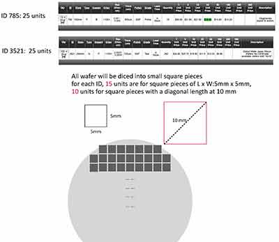
Reference #256758 for specs and pricing.
What is Scanning Electron Microscopy (SEM)? And What Wafers Should I Use?
A scientist was looking for the following:
Highly-Doped Silicon, P or N, no preference, The more doped, the better No preference in orientation Lowest resistivity Wafer thickness not critical DSP, highest grade polish.
These wafers will be used to deposit ceramics, so the surface properties are more critical than the semiconductor properties. We aim for a low-resistivity silicon to enable Scanning electron microscopy. Exact size is not so relevant as our sample holder is a rectangular shape, we'll have to cut it anyway.
If you have Gold or Platinum deposited on 1 or 2 sides of the wafer, it would be best, but we can otherwise deposit it ourselves.
UniversityWafer, Inc. Replied and Quoted:
We can supply the required materials in the form of wafers and we can also arrange to have them diced into 10×8mm chips. However, you have to specify how many wafers and/or Chips do you require. Unit price depends on the quantity ordered.
When you ask for Silicon Oxide wafers, what do you mean by that? - Here are some choices:
- Monocrystalline Quartz (SiO2) - this is the highest purity material - you must specify the crystallographic orientation (thermal expansion coefficient depends on crystal orientation)
- Fused Silica or Fused quartz (SiO2) - this comes in several grades differing primarily in light transmission at the far UV and IR wavelengths - Silicon wafers with Thermal Oxide layer (SiO2) on the surface, anywhere from 0.1 to 2.4µm thick (the Silicon wafer itself would be 300 to 1,000µm thick)
I would guess that Silicon wafer with Thermal Oxide layer is what you want for your ceramics research.
We can supply wafers with Platinum or Gold layer sputtered on them. You need to specify the thickness of Pt or Au layers (Pt & Au areexpensive).
Highly doped Silicon wafers have resistivity in the range (0.001-0.005)Ohmcm,
p-type would be Boron doped Si:B and n-type would be Arsenic doped, Si:As.
| Item | Material | Orient. | Diam. | Thick (μm) | Surf. | Res Ωcm | Comment |
| F863 | P/B | [100] | 4" | 525 | DSP | 0.001-0.005 | SEMI Prime, 1Flat, Empak cst, TTV<5μm, Free of striation marks |
| I135 | P/B | [100] | 4" | 500 | DSP | 0.001-0.005 | SEMI Prime, 2Flats, Empak cst, Wafers with striation marks |
| TS016 | P/B | [111] ±1° | 4" | 350 ±10 | DSP | 0.0039-0.0042 | SEMI Prime, 1Flat, Free of Striations, Empak cst |
| 6403 | N/As | [100] | 4" | 525 | DSP | 0.001-0.005 | SEMI Prime, 1Flat, Empak cst, TTV<5μm |
| B788 | N/As | [110] ±0.5° | 3" | 420 | DSP | 0.001-0.007 | SEMI Prime, in Empak, Primary Flat @ [1,-1,0] |
| TS018 | N/As | [100] | 6" | 575 ±15 | DSP | 0.0040-0.0041 | SEMI Prime, 2Flats (PF @ <110>±1°, SF 135° from PF}, Laser Mark, Empak cst |
| TS127 | N/As | [100] ±1° | 4" | 360 ±15 | DSP | 0.0054-0.0067 | SEMI Prime, 2Flats, TTV<5μm, Cassettes of 22 + 21 + 19 wafers |
Germanium Wafers for Imaging Silica Particles Using Scanning Electron Microscopy (SEM)
We are a small company that works in particulate control for ultra high purity water and chemicals. We are involved in a project which requires imaging silica particles using SEM. The commonly used Silicon wafers do not give us contrast for EDX. Hence, we are interested in evaluating Germanium wafers for this application. We would be interested in undoped, epitaxy ready, single side polished wafers of high purity to give the required contrast for EDX. Could you give us a section of wafer around 1 inch in dimension to see if your product is suitable for our purposes? I understand the wafers are quite expensive, so any broken/unsellable piece would do. I would also appreciate a detailed spec sheet and pricing information.
We do not have a orientation requirement. We don't want anything super thin, because we are interested in cleaving the wafers. But we dont want anything prohibitively expensive either in terms of thickness. To begin with, we need only a small portion (1" or lesser) for evaluation. At least 99.9% purity. We will need more wafers once we evaluate the wafer as suitable.
UniversityWafer, Inc. Quoted:
Germanium Wafer 25.4mm Undoped <100> 0.5mm SSP $Contact us Reference #241246
What Exactly Does Scanning Electron Microscopy (SEM) Do?
SEM is based on high-energy electrons emitted from the surface of the sample, which are exposed to high temperatures, high pressure and light. The interactions between electron beam and sample produce an image, similar to the way an optical microscope uses light to capture images. Depending on the electron microscope used, the image created can reveal details about the surface and the internal composition of a sample. Scanning electron microscopy can produce a wide range of images, such as images of biological samples and chemical compounds.
What Silicon Wafers Are Used for Scanning Electron Microscopy?
If you're interested in scanning electron microscopy, you're probably wondering: what silicon wafers are  used for scanning electron microscopy? In this article, we'll talk about the two main types, Si-III and Si-XII. Each is important for different kinds of applications, and we'll discuss the benefits of each one. But first, let's discuss what the differences are between these two types of silicon.
Si-III
SEM, also called scanning electron microscopy, is a technique that uses high-energy electrons emitted from the surface of a sample under high pressure, temperature, and light to create images. Unlike the optical microscope, which relies on light to generate images, SEM uses electrons to reveal detail on a sample's surface and internal composition. It is useful for studying biological and chemical samples.
X-ray diffraction images were also made on prototype silicon wafers for SEM. The Berkovich indents, which were placed far from the edge of the wafer, did not produce macroscopic cracks, and the lengths were only a few micrometres. In contrast, the bottom crack, shown in Figure 6b, ruptured the wafer. The tip of the lower crack has a high k value, which indicates it was the source of a fracture.
In SEM, crystalline silicon wafers are used as the sample substrate. The transparency and high atomic-plane structure of silicon wafers make them an excellent material for imaging small particles. Si-III silicon wafers are available in several shapes and sizes, including 4" (#16010), 5 x 7mm, and 10 x 10mm. It is also possible to use these wafers as substrates for AFM and atomic force microscopy experiments.
SEM images of ground-Si-III silicon wafers can reveal defects such as scratches and particles. A high-speed SEM microscope can achieve a high-feed rate without a burnt surface. It is possible to use deionized water as a coolant. The resulting images are extremely clear and detailed. They help researchers identify various defects in silicon wafers.
The spectral range of Si-III wafers allows scanning electron microscopy to analyze atomic and electronic structures in a variety of applications. Often, atomic-level details can be studied with this technique. The spectral range is 0.0506 nm. The Darwin width is 1.58 arc seconds. The wavelength corresponds to 7.6 x 10⁻⁶ radians.
During SEM, the image obtained by the spectroscopic analysis of silicon wafers is extremely high-resolution. This means that a single electron can examine multiple features at a time. The images gathered from scanning electron microscopy reveal the smallest details of the sample. Further, the SEM image can also show the size of the defect or crack. The size of the sample may vary due to the various processing methods applied to the silicon substrates.
A thin layer of silicon enables complete materials compatibility in the equipment. However, other wafer handling methods require adhesive materials and reduce thermal budget. Thin silicon wafers are too fragile for thermosonic bonding. Moreover, these techniques cannot work with ultrathin silicon wafers. A thin silicon ring supports the interior ultrathin silicon, which is transparent to red light.
SEM can be used to measure fine patterns on semiconductor wafers. In SEM, the electron beam used for the measurement is extremely low, with an energy of only 1keV. This lower energy ensures less damage to the sample. Improvement in magnification calibration ensures high-resolution imaging and a repeatability of less than one third of the measurement width. So, SEM is an excellent tool for studying fine details of complex samples.
The sample wafer is loaded into a wafer cassette. The wafer is then placed into the CD-SEM. A recipe is used to specify the dimensional measurements on the sample. The CD-SEM will automatically load and process the wafer, measuring the desired positions on the sample. Once measurements are complete, the sample is loaded back into the wafer cassette. A recipe is a collection of procedures, processing methods, and input data. The recipe specifies the measurements on the SEM image.
Scanning electron microscopy can also be used to examine the cracks around indents. Traditionally, the technique used a field emission electron microscope with an in-lens secondary electron backscattering detector. However, newer scanners have incorporated STEM (scanning transmission) and ion beam cannons into one system. These tools allow researchers to reconstruct cracks in three dimensions.
Si-XII
Si-XII silicon wafers for scanning electron microscopy have two main uses: as a substrate and for AFM experiments. They also allow for cleavage stepping across different atomic planes. To determine which one is better for scanning electron microscopy, two methods are used. The first technique uses hydrofluoric acid, and the second method uses sulfuric peroxide.
The dislocation image shows a narrow region where the crack is located. A wider region of the wafer contains a more complex fracture mechanism. This is triggered by a large strain field and a narrow crack tip. The width of the dislocation image is measured as a ratio of the tip to the length of the crack. The crack tip is approximately half the wafer's diameter, indicating that the silicon is not brittle enough to sustain large-scale strain fields.
The metalens design is highlighted in red dotted lines. This is a typical example of flat optic devices integrated on the same die. The SEM images in panels B and C are top views, while panel D shows a zoomed-in angled view of pillars near the edge of the metalens. The diameters change to accommodate the phase shift from 0 to 2p.
A two-mm-diameter metalens has a focal length of 1.732 mm and is composed of nanopillars. The metalens was fabricated on a 12-inch silicon wafer using a plasma-enhanced chemical vapor deposition method. A 600-nm a-Si layer was then deposited by ArF DUV immersion lithography. The metalens was subsequently placed into a scanning electron microscope imaging system and tested for imaging resolution. The minimum bar was 2.19 mm.
The TEM and SEM devices are similar, although they have their own limitations. In SEM, the electron beams are directed toward the sample while a light source enables the imaging of the specimen. The resulting image will be a magnified view of the sample's surface. The images will reveal the internal composition and surface details. SEM can also be used to examine biological samples and chemical compounds.
Another SEM technique is serial section transmission electron microscopy. This technique allows for the examination of large volumes, such as cells or tissues. The combination of serial sectioning and scanning electron microscopy on a conductive silicon wafer will allow for lateral pixel resolution of 3.7 nm. In this way, SEM can be performed on silicon wafers to determine the nature of molecules and cells.
Another method is to grind the Si-XII silicon wafers to get a pristine crystalline lattice. Si-XII silicon wafers are used for scanning electron microscopy and have a high-resolution surface. A newly developed diamond wheel containing ceria plays a significant role in obtaining a bright surface on Si wafers.
TEM uses Si-XII silicon wafers for the lateral face aperture. This aperture allows electron microscopic analysis of individual particles, vesicles, aerosol particles, and quantum dots. It also allows the study of functional particles. This is the preferred method for scanning electron microscopy. And in TEM, the electron microscope is used to look at functional particles like atoms and molecules.
High-fluence and low-fluence irradiation can increase the formation of Si-XII. They can also increase the melt depth. Both irradiation techniques are effective in improving the properties of silicon, as the resolidification-induced stresses result in pressure-induced plastic deformation. The second half of the thesis discusses optical hyperdoping of silicon. Pulsed laser irradiation is used to drive supersaturated concentrations of dopants into the semiconductor.