
Silicon Wafers for GaN and Silicon Transistor Integration
Silicon wafers provide a scalable platform for research involving GaN-on-silicon devices, silicon CMOS circuits, and heterogeneous transistor integration. Their availability in large diameters and compatibility with established semiconductor equipment make them useful for developing integrated power, radio-frequency, and mixed-signal devices.
GaN cannot normally be grown directly on bare silicon without carefully designed intermediate layers. Differences in lattice spacing and thermal expansion can produce stress, wafer bow, cracking, and crystal defects. GaN-on-silicon structures therefore commonly use nucleation, transition, and buffer layers between the silicon substrate and the active GaN device layers.
Selecting a Silicon Substrate
The appropriate silicon wafer specification depends on the GaN growth process, device architecture, and integration method. Important substrate parameters may include:
- Wafer diameter: Select a size compatible with the deposition and fabrication equipment.
- Crystal orientation: Si(100) is widely used in CMOS processing, while Si(111) is commonly selected for GaN epitaxy because its surface symmetry is more compatible with hexagonal GaN growth.
- Doping and resistivity: Electrical properties should be selected according to whether the substrate must provide conduction, isolation, or RF performance.
- Thickness and mechanical stability: Wafer thickness influences handling, thermal behavior, bow, and compatibility with high-temperature processing.
- Surface finish: Prime-grade polished surfaces are generally preferred for epitaxial growth and precision device fabrication.
- Flatness and bow: Low total thickness variation and controlled wafer bow help support uniform deposition, lithography, bonding, and alignment.
Integration Considerations
GaN and silicon transistors may be combined through direct GaN-on-silicon growth, wafer bonding, layer transfer, or advanced packaging. The best substrate specification depends on the selected method, the required thermal budget, and whether the finished device will be used for power switching, RF operation, sensing, or control electronics.
Tell us your required wafer diameter, crystal orientation, conductivity type, resistivity, thickness, surface finish, and quantity. We can help identify silicon substrates suitable for your GaN and silicon transistor research.
Get Your Silicon Wafer Quote FAST! Or, Buy Online and start researching today.
Stacking GaN and Silicon Transistors on Silicon Wafers
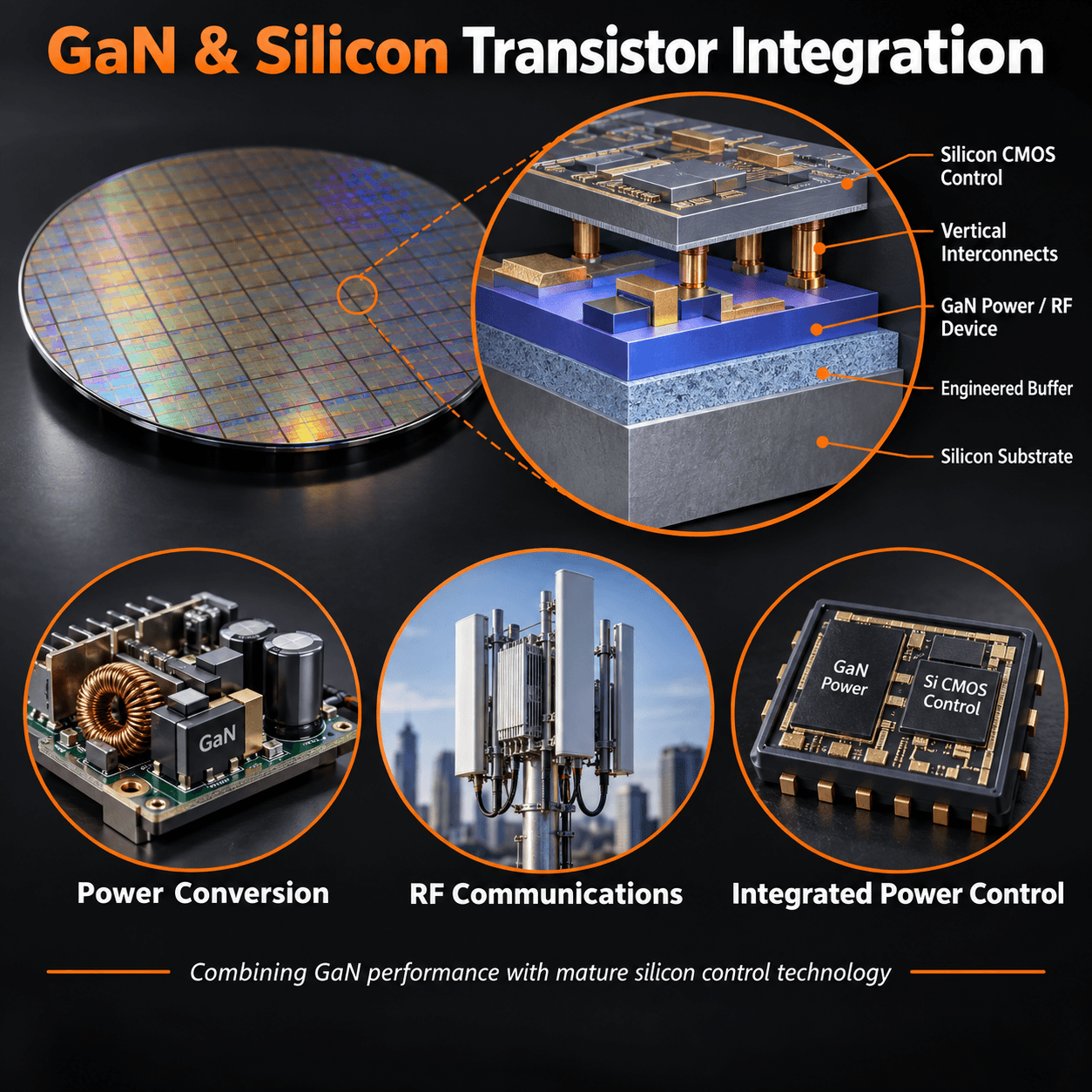
Combining gallium nitride (GaN) devices with conventional silicon transistors is an emerging approach to heterogeneous semiconductor integration. The goal is to place devices with different electrical strengths within the same package or vertically integrated structure.
GaN is a wide-bandgap semiconductor that can support high electric fields, high-frequency operation, and efficient power switching. Silicon remains the dominant material for complementary metal-oxide-semiconductor (CMOS) logic because its manufacturing processes are mature, scalable, and highly integrated.
Why Combine GaN and Silicon?
Integrating GaN power or radio-frequency devices with silicon control circuitry could reduce the distance between the switching device and its driver. Shorter electrical connections can decrease parasitic resistance and inductance, improve switching performance, and help create smaller power-management systems.
In a hybrid device, the GaN transistor may perform the high-voltage or high-frequency switching, while nearby silicon CMOS circuits provide control, sensing, protection, and signal-processing functions.
Approaches to GaN–Silicon Integration
GaN and silicon devices can be combined through several manufacturing approaches:
- GaN-on-Silicon Growth: GaN device layers are grown above a silicon substrate using engineered buffer layers that help manage lattice and thermal-expansion mismatch.
- Wafer or Die Bonding: Separately fabricated GaN and silicon device layers are bonded and electrically connected.
- Layer Transfer: A thin semiconductor layer is transferred onto another processed wafer to create a vertically integrated structure.
- Advanced Packaging: GaN and silicon dies are placed close together and connected using interposers, redistribution layers, or other low-parasitic packaging technologies.
Potential Applications
GaN–silicon integration is being investigated for applications that benefit from efficient power switching, high-frequency operation, and compact control electronics, including:
- Power converters and voltage regulators
- Electric-vehicle power electronics
- Data-center and telecommunications power supplies
- Radio-frequency amplifiers and communication systems
- Compact power-management integrated circuits
- High-frequency and mixed-signal semiconductor research
Why Use Silicon Substrates?
Silicon wafers are available in large diameters and are compatible with established semiconductor fabrication equipment. This makes silicon an attractive platform for research into scalable GaN integration and potentially lower-cost device manufacturing.
However, directly growing GaN on silicon presents technical challenges. Differences in lattice spacing and thermal expansion can introduce stress, wafer bow, cracking, and crystal defects. Engineered nucleation and buffer layers are therefore commonly used between the GaN device structure and the silicon substrate.
Thermal and Process Challenges
Thermal management is especially important in vertically integrated devices. Closely stacked active layers can create concentrated heat that must be removed without damaging the devices or reducing reliability. Researchers must also ensure that later fabrication steps do not exceed the temperature limits of previously completed transistors and metal interconnects.
GaN and silicon transistor stacking remains an active research and development field. Successful integration could combine the power and high-frequency capabilities of GaN with the control density and mature manufacturing infrastructure of silicon CMOS.