Indium-Tin-Oxide (ITO) Coated Substrates For Ellipsometric Research
Typical researchers quote request:
Reference #100034 for specs and pricing.
Buy ITO Substrates Online and Save!
Indium Tin Oxide Substrates to Study Deformable Mirror for Adaptive Optics Applications
A university scientist requested the following:
I'm conducting research that requires the use of photoconductors, and I would like to ask if it would be possible to have a layer of indium tin oxide (ITO) deposited on one side of the wafer.
I am working on a device used as a deformable mirror for adaptive optics applications.
I am in the early phase of my work, and I need materials such as silicon, gallium arsenide,
and zinc selenide.
Requirements: high resistivity, thickness < 3 mm, round shape, lapped both sides, and ITO coating.
Reference #246503 for specs and pricing.
Get Your Quote FAST! Or Buy Online and Start Researching Today!
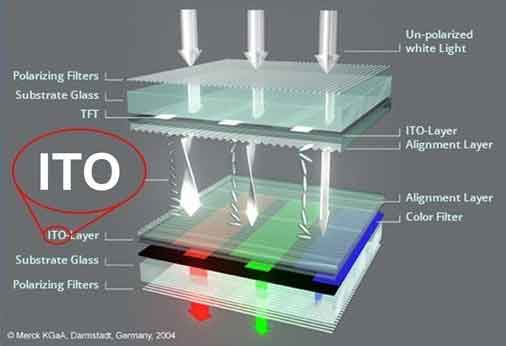
What is Indium Tin Oxide on Glass?
Indium tin oxide (ITO) on glass is a thin film of indium oxide and tin oxide deposited on a transparent substrate. It provides excellent optical transparency and electrical conductivity, making it widely used in displays, optoelectronics, and sensors.
ITO is typically deposited using sputtering or PVD to ensure uniform thickness and high stability, even under vacuum or elevated temperatures.
ITO Glass for Resistive Anode Detector
Question:
I'm reaching out regarding ITO Glass squares. I am evaluating them for a resistive anode detector and need to confirm porosity for vacuum use.
Size requested: 100 × 100 mm, 15–20 ohm/sq.
Answer: ITO sputtered at elevated temperature is dense, non-porous, and fully stable under vacuum.
Reference #273659 for specs and pricing.
At What Temperature Do ITO Glass Wafers Start Degrading?
ITO glass can withstand temperatures up to ~200°C.
Optical/electrical drift may begin around 90°C depending on thickness and deposition method.
Reference #272563 for specs and pricing.
ITO Glass Specifications
• Glass / SiO₂ buffer (~23 nm) / ITO
• Sputtered deposition
• Photolithography patterning available
• Sheet resistance: 6 – 250 ohm/sq
• Thickness options: 0.4 – 1.1 mm
ITO Plastic Film
Polyethylene terephthalate (PET) substrates coated with ITO. Ideal for flexible electronics and transparent heaters.
PEN / ITO
• Magnetron sputtered ITO
• Patterning via lithography or laser
• Sheet resistance: 6 – 500 ohm/sq
• Substrate thickness: 0.125 – 0.21 mm
• Transmission: > 85%
Pilkington FTO Glass (TEC Series)
• 15 ohm/sq FTO
• Thickness 3.2 mm
• Transmission > 82%
• Size: 50 × 50 mm
Nippon Sheet Glass FTO
• Sheet resistance < 7 and < 13 ohm/sq
• Sizes up to 300 × 300 mm
Normal FTO Glass
• Made in PRC
• Sizes up to 300 × 300 mm
• Sheet resistance < 15 ohm/sq
Indium Tin Oxide Material Explained
Indium Tin Oxide Coated Glass for Sale
- ITO coated glass
- ITO-coated plastic films (PET, PEN)
- FTO coated glass
- ITO cleaning detergents
ITO Glass Sizes Include:
- 300 × 400 mm
- 400 × 500 mm
- 450 × 550 mm
ITO Glass Slide Sizes
- 25 × 25 mm
- 25 × 75 mm
- 50 × 75 mm
ITO Coating Services on Silicon Wafer
A researcher requested an ITO coating on silicon wafers along with a graphite or graphene oxide coating on the reverse side. These applications involve optoelectronic activation by laser illumination.
Reference #228263 for coating specifications.
ITO Glass Substrates Used for Electroadhesion
Electroadhesion researchers requested a stack of Glass + ITO + dielectric layer (<1 μm).
Dielectric coatings with high breakdown strength are available upon request.
Reference #276257 for specs and pricing.
What is Indium Tin Oxide (ITO)?
Indium tin oxide is a solid solution of indium(III) oxide and tin(IV) oxide with unique transparent semiconductor
properties. The material is widely used in thin-film electronics, sensors, display technologies, and photonics.
ITO Layers
ITO has a melting point near 2800°F. Its common composition is represented as In₄Sn. As an n-type semiconductor with a large
~4 eV bandgap, it is a preferred material for transparent electronics such as touchscreens.
Because of its strong conductivity and transparency, ITO is often used for EMI shielding, solar cells, transparent electrodes,
and optical devices requiring both electrical and optical performance.
Its low surface resistance and high film uniformity make it a high-value material for scientific and industrial use cases.
What ITO Specs Do I Use to Fabricate an Electrostatic Actuation System?
A scientist requested the following:
150 mm × 150 mm ITO glass substrates
with thickness ≤ 0.7 mm and surface resistivity ≤ 10 ohm/sq.
Indium tin oxide is a ternary compound composed of indium, tin, and oxygen. Its bulk form appears grey–yellow and
metallic. Due to its conductivity and transparency, ITO is commonly used in microelectronic systems.
ITO’s large bandgap (~4 eV) and high electrical conductivity make it ideal for electrostatic actuation, printable
electronics, and touch-sensitive devices.
What ITO Wafers Are Used for High-Power Lasers & Electro-Optics?
A research group requested ITO wafers for high-power laser and 3D printing optical applications. Their ideal size
was 40 × 40 × 2 mm (1 mm acceptable as alternative).
Available configuration:
• 20 ohm/sq ITO on polished glass
• Japan display grade substrate
• Size: 40 × 40 × 1.1 mm
ITO Compatibility with High-Power Lasers and Electro-Optics
Indium Tin Oxide wafers are widely used for optical modulation and plasmonic tuning applications.
Carrier-dependent refractive index control allows ITO to be engineered for specific photonic functions.
Indium Tin Oxide Market Trends
Demand for ITO continues to grow due to its unique optical and electrical characteristics. Applications include
transparent heaters, flexible electronics, photodetectors, and display technologies.
ITO Coated PET Film
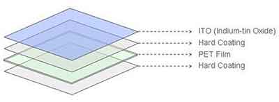
ITO-coated PET sheets offer high transparency and electrical conductivity. They are used in flexible displays,
solar cells, and thin-film printed electronics.
Is Indium Tin Oxide (ITO)  Conductive?
Yes — ITO is highly conductive while retaining optical transparency. This makes it useful in displays,
photovoltaics, sensors, and MEMS devices.
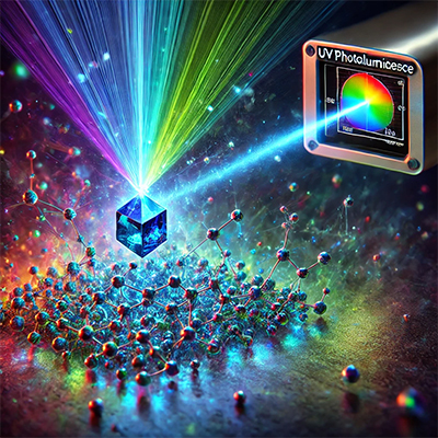
Indium Tin Oxide (ITO) UV Photoluminescence Data
A research scientist requested UV photoluminescence data for ITO-coated SiO₂ wafers.
Sample sizes: 4" diameter, 0.7 mm and 1.1 mm thickness.
UV Photoluminescence (UV-PL)
UV-PL is used to evaluate optical and electronic properties of semiconductors.
It measures emitted light after UV excitation.
- Excitation: UV laser or lamp excites electrons.
- Absorption: Electrons jump to conduction band.
- Emission: Recombination produces luminescence.
- Analysis: Spectrum reveals material properties.
- Bandgap measurement
- Defect identification
- Thin-film quality analysis
- Optoelectronic device evaluation