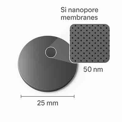
Do you sell 25 mm in diameter Si nanopore membranes with a pore size of 50 nm?
Silicon Nanopore Membranes
A nano-materials research chemist requested a quote for the following.

Reference #323617 for specs and pricing.
Get Your Quote FAST! Or, Buy Online and Start Researching Today!
Recent Nanopore Membrane Requests
- I'm interested in a custom 25 mm diameter silicon or silicon nitride membrane with 50 nm pore size for [brief description of your application—e.g., filtration, TEM support, optics]. Could you provide pricing, lead time, and technical specs?
- I'm looking for your nanoporous silicon nitride membrane chips with ~50 nm pore diameter. Could you share product variants, price, availability, and typical shipment time to the U.S.?
- I’d like to request a quote for a custom silicon nitride membrane window, 25 mm diameter, ~50 nm pores. Could you provide details on pricing, manufacturing lead time, and any technical datasheets available?
What Are Nanopore Membranes?
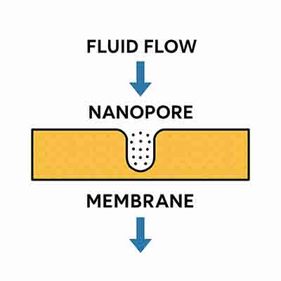
Nanopore membranes are thin, solid-state or biological films containing tiny holes (pores) at the nanometer scale that can selectively allow molecules, ions, or fluids to pass through. They are widely used in nanotechnology, biotechnology, and materials science because their pore size and surface chemistry can be precisely engineered.

Here’s a breakdown:
Structure
-
Membrane material: Can be silicon, silicon nitride, graphene, polymer films, or biological lipid bilayers.
-
Pores: Typically 1–100 nanometers in diameter, but their size and geometry can be tailored.
-
Thickness: Often just tens to hundreds of nanometers thick, enabling high sensitivity.
Key Properties
-
Size-selectivity: Only particles smaller than the nanopore can pass through.
-
Electrical sensitivity: Changes in ionic current across a pore can reveal the passage of single molecules.
-
Surface tunability: Pore walls can be chemically modified to control interactions with analytes.
Applications
-
DNA/RNA Sequencing
Nanopore membranes are used in sequencing devices (e.g., Oxford Nanopore), where single DNA strands pass through a pore and changes in electrical current are measured to identify bases. -
Biosensing
Detecting proteins, viruses, or small molecules by monitoring how they alter ionic current as they interact with or pass through the nanopore. -
Filtration & Separation
Selective filtration of gases, ions, or molecules (e.g., water purification, desalination, protein separation). -
Energy Devices
In batteries and fuel cells, nanopore membranes can regulate ion flow, improving performance and safety.
Research Applications and Commercial/Industrial Uses
🔬 Research & Academic Applications
-
DNA/RNA Sequencing
-
Solid-state nanopores (SiN, graphene) or protein nanopores (like α-hemolysin) allow individual nucleotides to be detected by measuring ionic current.
-
Oxford Nanopore Technologies has made this commercially available for portable sequencing.
-
-
Single-Molecule Biosensing
-
Proteins, viruses, and nanoparticles can be identified by their unique electrical “signatures” as they pass through a pore.
-
Useful in diagnostics, virology, and proteomics research.
-
-
Nanofluidics
-
Studying how fluids behave when confined to nanoscale channels.
-
Reveals new physical chemistry phenomena such as altered viscosity, ion transport, and surface interactions.
-
-
Drug Delivery Models
-
Nanopores help study how drugs diffuse across membranes, mimicking biological barriers (e.g., blood–brain barrier).
-
🏭 Commercial & Industrial Applications
-
Water Purification & Desalination
-
Nanopore membranes can filter salts, heavy metals, and organic molecules with high selectivity and efficiency.
-
Graphene oxide membranes are particularly promising here.
-
-
Gas Separation
-
Nanopores can separate gases (e.g., CO₂ from CH₄, hydrogen purification).
-
Useful in energy production and carbon capture.
-
-
Batteries & Fuel Cells
-
Nanopore separators help regulate lithium-ion transport in batteries.
-
Can prevent dendrite growth in Li-metal batteries, improving safety and lifetime.
-
-
Medical Diagnostics
-
Point-of-care devices use nanopore membranes to detect biomarkers in blood or saliva.
-
Potential for low-cost, portable diagnostic kits.
-
✅ In short:
-
In research, nanopore membranes are prized for high-resolution sensing at the single-molecule level.
-
In industry, they are valued for separation, filtration, and ion regulation in water, energy, and healthcare applications.
Silicon Nitride (SiN) Nanopore Membranes for Superfluid Helium Experiments
A low-temperature physicist requested a quote for the following.
I am a low-temperature physicist working with superfluid helium, and I am interested in your capabilities. What is the smallest pore size you can reliably make (array or single hole), and what would be the corresponding thickness of the SiN membrane? For my purposes I would need a window size on the order of microns or larger.

UniversityWafer, Inc. Replied:
We can support both single-aperture and arrayed pores in low-stress LPCVD silicon nitride (SiN) membranes. Below are our typical, reliably manufacturable ranges; if your needs fall outside these, we can review as a custom run.
Pores
-
Single hole (TEM-drilled): ~3–10 nm (tight tolerance), 10–50 nm (very robust yield).
Typical diameter tolerance: ±1–2 nm (≤20 nm pores) or ±10% (>20 nm). -
Arrayed pores (e-beam + RIE / HIM): ~20–50 nm (high yield), 50–200 nm (very robust), with pitches ≥2× diameter.
Array areas from tens of µm² up to mm² are feasible.
SiN membrane thickness (LPCVD, low-stress)
-
Standard: 20, 30, 50, 75, 100, 200 nm (others on request).
-
Guidance: For ≤20 nm pores we usually recommend 30–75 nm membranes; for 50–200 nm pores, 50–200 nm membranes give excellent robustness.
Window (clear aperture) size
-
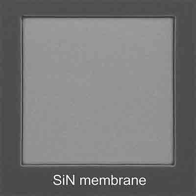
We can provide free-standing SiN “windows” from a few microns across up to ≥1 mm on Si frames.
-
For “micron or larger” windows as you mentioned: 10–200 µm is straightforward; 200 µm–1 mm is also common with appropriate thickness and frame design.
Substrate & frame
-
Si frames: 200–500 µm thick, standard die sizes (e.g., 3×3 mm to 10×10 mm; larger on request).
-
Through-wafer openings are KOH/DRIE-defined; we can include vent features for vacuum compatibility.
Surface & compatibility options
-
ALD overcoats (Al₂O₃, HfO₂) to tune wetting and reduce pinhole risk.
-
O₂ plasma clean and particle-controlled packaging.
-
Alignment marks for your downstream lithography.
-
Optional gold perimeter pads for indium sealing/thermal anchoring.
Metrology & QC
-
SEM images of representative pores (or every device for single-aperture runs), thickness ellipsometry, membrane bow/defect screening.
-
Electrical leak/withstand tests or helium leak checks available on request.
If you share the items below, I’ll send back a concrete spec and quote:
-
Target pore diameter(s) and tolerance; single or array (give array area, pitch, and count)
-
Preferred SiN thickness and acceptable range
-
Window (clear aperture) size(s) and frame (die) size
-
Substrate thickness and any mounting/seal requirements (e.g., indium, CF flange)
-
Surface/ALD requests and cleanliness level (e.g., low-outgassing, cryo-ready)
-
QC you’d like documented (SEM count, leak limits, etc.) and desired yield
-
Quantity and delivery timeline
Best,
[Your Name]
Practical guidance for your use case (superfluid helium)
-
Single weak-link studies: A 10–50 nm diameter, 30–75 nm thick SiN is a sweet spot (stiff yet short “channel”) and TEM drilling gives the cleanest geometry.
-
Arrayed flow experiments: 20–100 nm pores on 50–100 nm SiN with pitches ≥2× diameter keeps membranes robust over 100–500 µm windows.
-
Larger window wants: If you truly need ≥500 µm windows and ≤20 nm pores, lean thicker (≥75–100 nm) or use a tiled design (multiple smaller windows per die).
-
Cryo mechanics: Low-stress LPCVD SiN handles repeated cooldowns well; keep aspect ratio (thickness:window size) conservative to minimize bowing. Consider ALD Al₂O₃ if you want more controlled wetting or to “pin” surface states.
-
Cleaning: Prefer O₂ plasma/UV-ozone before cooldown; avoid aggressive wet cleans that can roughen sub-20 nm pores.
Quick capability matrix (what you can safely quote as “reliable”)
-
Single pore (TEM-drilled): 3–10 nm (tight), 10–50 nm (robust)
-
Array pores: 20–50 nm (high yield), 50–200 nm (very robust)
-
SiN thickness: 20–200 nm standard (thicker on request)
-
Window (clear aperture): 10 µm → 1 mm (design-dependent)
-
Tolerances: ±1–2 nm (≤20 nm), else ±10% typical
-
Metrology: SEM, ellipsometry, defect/bow screening; leak tests on request
If you want, I can turn this into a one-page PDF capability sheet and a quote request form you can send to multiple fabs.
