
What is a Silicon Wafer Chip?
A silicon wafer chip is a thin piece of semiconductor material, typically silicon, that is used in the fabrication of microelectronic devices such as transistors, integrated circuits, and microprocessors. The wafer is typically a few hundred micrometers thick and can be as large as a few inches in diameter. The silicon is carefully processed and polished to create a smooth, uniform surface on which the microelectronic devices are built. Silicon wafer chips are a critical component of the electronics industry and are used in a wide range of applications, including computers, smartphones, and other electronic devices.
Get your Silicon Wafer Quote FAST! Or, Buy Si Online and Start Researching Today!
How to Create a Silicon Wafer Chip
Creating a silicon wafer chip can be a complicated process. However, there are a few different techniques that can be used to help you get started.
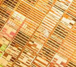
What Chips Look Like On a Silicon Substrate
Dopants added to silicon wafers
During the growing process of a silicon wafer, dopants are added to improve its properties. The type of dopants used depends on the purpose for which the wafer is used. Dopants can be used to increase or decrease the concentration of free electrons in the silicon crystal. The doping process also changes the electrical properties of the semiconductor region.
In the doping process, the impurity atoms are deposited onto the surface of the silicon wafer. This is done by heating the silicon to the requisite temperature. Once the heat is removed, the dopant atoms are transported to the silicon surface. These dopants are accelerated by an electric field to high energy levels. Once the dopant atoms are on the surface of the silicon wafer, they are subsequently irradiated. Depending on the method, dopant ions are masked by a thick material.
This type of doping can be used for lowering the free electrons in silicon and improving the electrical conductivity of the wafer. It also allows doping with acceptors and donors. In addition, doped semiconductors are much more efficient than undoped ones.
Ion implantation is the primary technology for introducing dopants into silicon wafers. It provides a well-controlled concentration of dopants. This process involves a series of steps including prebaking, ion implantation, thermal annealing, and postimplantation. Dopant concentration is increased to a level that is high enough to allow ionization of practically all dopant atoms. This is followed by thermal annealing to activate the dopant.
Another type of doping technique uses a planar dopant source. This is a new, defect-free, and reproducible solid-source doping process. The source can be a rigid holder wafer with CVD doped oxides or a spin-on dopant. The source is placed in close proximity to the wafer and the dopant is injected.
The dopants can be masked by a thick material, such as aluminum oxide. The masked regions are further doped by ion implantation. This is a new method for dopant diffusion into silicon wafers. It avoids channeling effects and enables the formation of shallow junctions. It is a good candidate for producing high-performance devices.
During the process of dopant diffusion into a silicon wafer, the dopants are rearranged in the crystal. This leads to a silicon wafer that is a lot more conductive than an un-doped one.
Bonding process to bond top dies 18 to bottom wafer 10
Among the many things that the semiconductor industry is now doing, wafer level packaging is one of the most important. This technology can package 50,000 devices at once. It also helps to improve size, cost, and reliability.
While there are several methods of bonding, the most common is by using a polymer adhesive. The adhesive is formed into a pattern that matches the shape of the die. Once the adhesive cures, the second die can be attached.
The first step in the process is to secure the substrate to an unheated workstage. Next, a high voltage is applied across the two wafers. This causes the ion migration that will eventually lead to a strong bond. This is achieved through a sophisticated vision system that can inspect the dispensed pattern.
The first thing to note is that the adhesive is contained in a reservoir. It is then fed into the dispensing mechanism. It is then dispensed in a pattern that matches the size of the chip. It is then heated to a temperature of around 350 to 450 degC. Silver particles are then added to the compound to boost electrical conductivity.
The second step is to use a chemical mechanical polishing tool to polish the copper pads on the wafer. These can be tricky to handle, so special tools are needed to hold the die flat against the substrate.
The third step is to use a vacuum pick up tool to pick up the die from the wafer. The vacuum will then push the aligned die onto a pre-dispensed bond position. This may sound straightforward, but a poorly placed die can cause an epoxy bleed out. This is not the only reason why a controlled die pick up procedure is necessary.
The last step is to use a thermal budget to determine the most appropriate temperature for bonding. For example, the correct temperature for a high-power RF amplifier requires a very small and constant bond line thickness.
There are four main die attach processes used in semiconductor packaging. The most common is by using a polymer or epoxy adhesive. The other three are by using a structured, wafer-level or cavity-based bonding method.
Wire bonding or flip-chip techniques for silicon wafer chip
Various wire bonding or flip-chip techniques for silicon wafer chip have been developed by the electronics industry. These techniques offer a number of advantages over conventional methods. They also provide an opportunity to optimize the performance of microelectronic circuits. They can be applied to a variety of products.
Most wire bonds are made using gold, copper, or aluminum. This material provides a good path for heat dissipation and strain relief. They can be anisotropically conductive or isotropically conductive. They are used in consumer electronics as well as in mainframes.
The most common wire bonding techniques include ball and wedge bonding. These methods are based on compliant wires. A compliant wire provides a strain relief that minimizes mechanical stress.
Thermocompression bonding is an alternative method. It involves pressing a wire and heating the semiconductor surface. This technique is developing in popularity and generates an excellent physical bond. It also reduces the likelihood of cracking. It requires 5,000 to 10,000 pounds of force per square inch.
Thermosonic bonding involves pre-heating a lead wire. Then, the wire is subjected to vibration energy. This helps to shape the bond between the wire and the bond pad. The result is a delicate bond wire.
Thermocompression bonding can be more expensive than the ball and wedge bonding methods, but it offers improved reliability. It also requires the use of a polymer underfill material that reduces the overall amount of thermomechanical stress. This is important to chip packaging.
Plasma cleaning is another technique used to improve interfacial adhesion for chip packaging. This process removes fluoride and oxide contamination from the chip's surface. This technique may not be suited for thick organic contamination.
The process of forming a flip chip requires a special machine. This machine heats up the chip and substrate. The chip is then aligned upside down. It is then bumped with a conductive material. The resulting contact area is then metalized. This creates a reliable interconnect.
The process of assembling a flip chip is similar to a traditional IC fabrication process. The main advantage of this method is that it significantly lowers the size and weight of the device.
Die attach pads on silicon wafer
Increasing complexity and growing demand for hand-held electronic devices has spurred greater use of 2.5D and 3D packaging. This has created challenges for die attach. These techniques use adhesives and films to attach silicon chips to substrates. It is important to understand how these techniques work, as they can have a significant impact on the final product and process performance.
Wire bonding is a traditional interconnect technique that has been used in volume production for years. This process involves introducing a small amount of solder onto a bonding pad. The die is then reflowed and bonded to the pad. The result is a very strong bond. The molten solder exerts pressure on the die, exerting forces that create the bond.
There are two types of die attach: epoxy and eutectic. Epoxy is the most common type, and 70 to 80 percent of current manufacturers use this method. This is due to its high die bonding stability and compatibility with dicing tape. However, it is not recommended for die that contain solderable metals.
Another type of die attach is no-flow. This is a more efficient process, which allows for a thinner die. It also allows for a smaller leadframe pad. This type of attachment is suitable for ultra thin wafers.
Other types of die attach include flip chip, area array interconnect and direct mechanical contact. These methods all require special equipment to perform the process. These processes are very different from each other, and each uses different materials. They are also different in their workflow procedures. The benefits of each method vary, but they all offer unique advantages.
The first is that the bonding pads are raised slightly above the surface of the die. This interface allows for mono-metalic bonding, enabling more compact die packages. It can also be used for a variety of applications, including a chip-stack bonding method.
The second advantage of eutectic die attach is that it does not introduce solder or outside adhesive to the die. It can be performed with a much shorter heat ramp up and down cycle. In addition, the backside of the die can be contacted for thermal management and conductivity.