
"We are developing high-speed infrared photodetectors and require double-side polished germanium wafers with a <100> orientation. Could you provide availability, resistivity options, wafer thicknesses, and pricing for prototype fabrication? We are also interested in custom wafer diameters if available."
Get Your Germanium Wafer Quote FAST!
UniversityWafer supplies electrical-grade and optical-grade germanium wafers (Ge wafers) for semiconductor research, infrared optics, photonics, detectors, and advanced electronic devices. Our custom wafers are available in a wide range of diameters, crystal orientations, dopant types, resistivity ranges, thicknesses, and polished surface finishes to meet your exact research or production requirements.
Recent Research Inquiry
Custom Germanium Wafer Options
- Electrical-Grade and Optical-Grade Germanium for semiconductor and infrared applications.
- Undoped, N-Type, and P-Type substrates with custom resistivity specifications.
- <100>, <111>, <110>, and custom crystal orientations.
- Single-Side Polished (SSP) and Double-Side Polished (DSP) surface finishes.
- Custom diameters from research-scale wafers through production sizes with precision edge profiles.
- Standard and custom wafer thicknesses for detector, photonic, and microelectronic applications.
- Research quantities, prototype lots, pilot production, and high-volume manufacturing.
Applications
Our germanium substrates are commonly used for photonic devices, photodetectors, multi-junction solar cells, infrared optical components, thermal imaging systems, radiation detectors, high-speed electronics, and advanced semiconductor research. Our engineering team can recommend the ideal wafer specifications for your application.
Get Your Germanium Wafer Quote FAST! Or, Buy Online and Start Researching Today!
Why Choose Germanium Wafers?
Germanium wafers (Ge wafers) are widely used in advanced semiconductor research because of their high electron and hole mobility, excellent infrared transmission, and compatibility with silicon-based device fabrication. Germanium substrates are ideal for applications in photonics, infrared optics, high-speed electronics, solar cells, and radiation detectors.
UniversityWafer supplies electrical-grade and optical-grade germanium wafers in a variety of diameters, crystal orientations, dopant types, resistivity ranges, and polished surface finishes. Whether you require a single prototype wafer or production quantities, we can manufacture germanium substrates to your exact specifications.
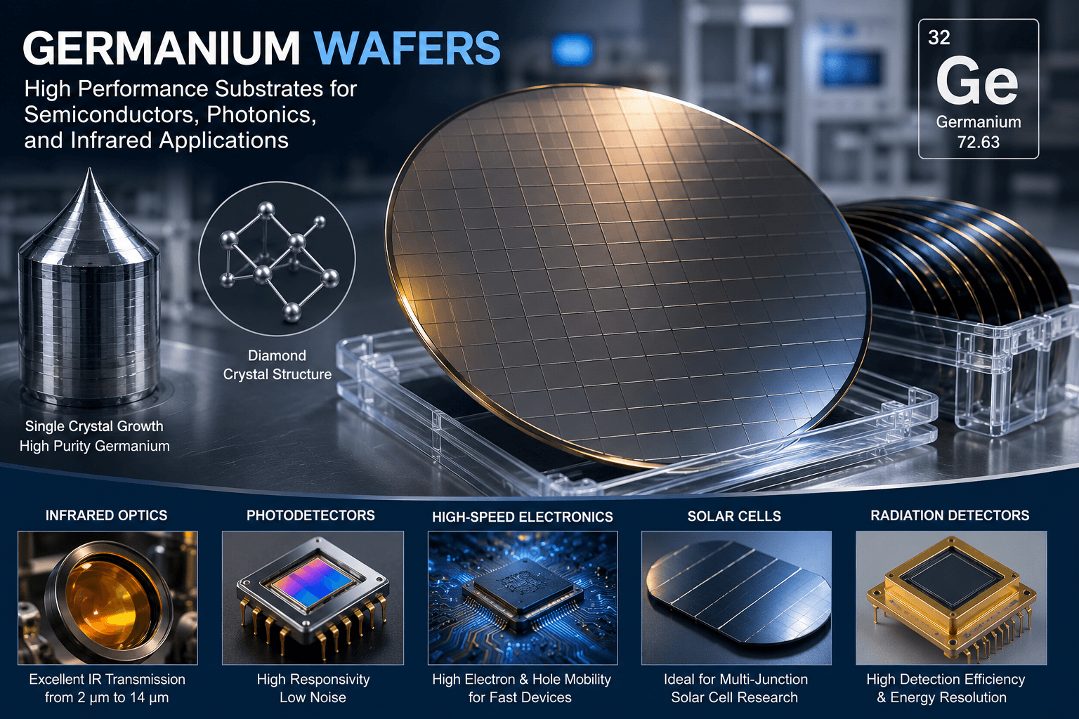
Germanium Wafer Specifications
| Specification | Available Options |
|---|---|
| Diameter | 2", 3", 4", 6", 8" and custom sizes |
| Crystal Orientation | <100>, <111>, <110> and custom orientations |
| Dopant Types | Undoped, N-Type, P-Type |
| Surface Finish | Single-Side Polished (SSP) or Double-Side Polished (DSP) |
| Resistivity | Research-grade and production-grade specifications |
| Thickness | Standard and custom thicknesses available |
Applications of Germanium Substrates
- Infrared optics and thermal imaging systems
- High-speed semiconductor devices
- Photodetectors
- Multi-junction solar cells
- Infrared cameras and optical windows
- Fiber-optic communication devices
- Radiation detectors
- MEMS and sensor development
- Thin-film epitaxy research
- Advanced semiconductor device fabrication
Why Researchers Choose UniversityWafer
For more than two decades, UniversityWafer has supplied germanium substrates to universities, government laboratories, and semiconductor manufacturers worldwide. Our experienced engineering team can recommend the appropriate wafer diameter, crystal orientation, dopant type, resistivity, thickness, and surface finish to meet your research or production requirements while providing fast quotations and dependable worldwide delivery. We also supply complementary silicon wafers, GaAs wafers, SiC wafers, and GaN substrates for advanced semiconductor research.
Related Germanium & Semiconductor Resources
- Photodetector Wafers – Substrates for infrared, visible, and ultraviolet photodetector research.
- Photonics Research Substrates – Materials for integrated photonics and optical device fabrication.
- Solar Cell Wafers – Semiconductor substrates for photovoltaic and multi-junction solar cell research.
- Silicon Wafers – Prime, test, and custom silicon wafers for semiconductor fabrication.
- Silicon Epitaxial Wafers – Epitaxial substrates for CMOS, MEMS, and advanced device development.
- Silicon-on-Insulator (SOI) Wafers – High-performance substrates for MEMS and integrated circuits.
- Gallium Arsenide (GaAs) Wafers – Compound semiconductor substrates for RF, microwave, and optoelectronic devices.
- GaN on Sapphire Wafers – Wide-bandgap substrates for LEDs, power electronics, and UV photonics.
- Silicon Carbide (SiC) Wafers – High-temperature and high-power semiconductor substrates.
- Zinc Selenide (ZnSe) – Infrared optical material for CO₂ laser systems and thermal imaging.