
High-Quality Graphene Wafers for Research & Development
Graphene wafers are among the most promising materials in modern materials science due to their remarkable combination of electrical conductivity, mechanical strength, optical transparency, and thermal conductivity. UniversityWafer supplies premium-quality graphene materials for universities, national laboratories, semiconductor manufacturers, and research organizations developing next-generation electronic, photonic, and sensing technologies.
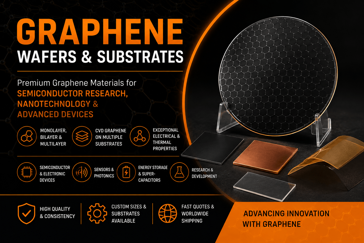
Our selection includes monolayer, bilayer, trilayer, and multilayer graphene wafers, along with graphene oxide (GO) and reduced graphene oxide (rGO). These materials are available on a variety of substrates including silicon, SiO2/silicon, copper, quartz, sapphire, PET, and other specialty materials to support both fundamental research and commercial device development.
Applications of Graphene Wafers
- Semiconductor device research
- Flexible and wearable electronics
- Field-effect transistors (GFETs)
- MEMS and NEMS devices
- Photonic and optoelectronic devices
- Biosensors and chemical sensors
- Energy storage and supercapacitors
- Transparent conductive electrodes
- Quantum materials research
- University and government laboratory research
Custom Graphene Solutions
UniversityWafer provides custom graphene solutions tailored to your research requirements, including wafer diameter, substrate material, graphene layer thickness, transfer methods, and surface preparation. Whether you require small prototype quantities or production-scale volumes, we can help identify the ideal graphene substrate for your project.
Get Your Graphene Wafer Quote FAST! Or Buy Online and Start Researching Today!
Why Choose UniversityWafer?
For decades, UniversityWafer has supplied premium research substrates and advanced materials to scientists and engineers worldwide. Our graphene products are manufactured to demanding quality standards and supported by expert technical assistance, competitive pricing, fast quotations, and worldwide shipping to accelerate your research and development efforts.
What Is a Graphene Wafer?
A graphene wafer is a substrate coated with one or more atomically thin layers of graphene—a two-dimensional sheet of carbon atoms arranged in a hexagonal lattice. Just one atom thick, graphene exhibits extraordinary electrical conductivity, exceptional carrier mobility, outstanding mechanical strength, and excellent thermal conductivity. These unique properties make graphene one of the most extensively studied materials for next-generation semiconductor devices, flexible electronics, photonics, quantum technologies, and energy storage systems.
Graphene can be synthesized using several techniques, with chemical vapor deposition (CVD) being the most common method for producing large-area, high-quality graphene films. After growth, graphene is transferred onto substrates such as silicon, silicon dioxide (SiO2), quartz, sapphire, copper, or flexible polymers depending on the intended application.
Available Graphene Materials
| Material | Description & Typical Applications |
|---|---|
| Monolayer Graphene | Single-atom-thick graphene for high-speed electronics, photonics, and quantum research. |
| Bilayer Graphene | Two graphene layers offering tunable electronic properties for advanced semiconductor devices. |
| Trilayer & Multilayer Graphene | Additional graphene layers providing enhanced durability and specialized electrical characteristics. |
| Graphene Oxide (GO) | Oxygen-functionalized graphene used in sensors, membranes, biomedical research, and composite materials. |
| Reduced Graphene Oxide (rGO) | Partially restored graphene with improved conductivity for energy storage and electronic applications. |
Key Material Properties
- Exceptional electrical conductivity
- Very high electron mobility
- Outstanding thermal conductivity
- High optical transparency
- Excellent mechanical strength and flexibility
- Large surface area for sensing applications
- Atomically smooth surface
- Compatible with semiconductor fabrication processes
Research & Industrial Applications
Graphene continues to drive innovation across numerous scientific and industrial fields. Researchers use graphene wafers for field-effect transistors (GFETs), MEMS and NEMS devices, biosensors, photodetectors, transparent conductive electrodes, flexible displays, quantum computing, RF electronics, batteries, supercapacitors, and advanced composite materials. Its exceptional combination of electrical, optical, and mechanical properties makes graphene an ideal platform for developing next-generation technologies.
UniversityWafer supplies premium research substrates and high-quality graphene wafers in a variety of layer counts, substrate materials, and custom specifications to support semiconductor research, nanotechnology, photonics, and advanced materials development.