
Custom Solar Cell Wafers & Photovoltaic Substrates
UniversityWafer supplies premium solar cell wafers and photovoltaic substrates for universities, national laboratories, renewable energy companies, and semiconductor manufacturers. Whether you are developing prototype photovoltaic devices or scaling toward production, we provide research-grade substrates manufactured to your exact specifications.
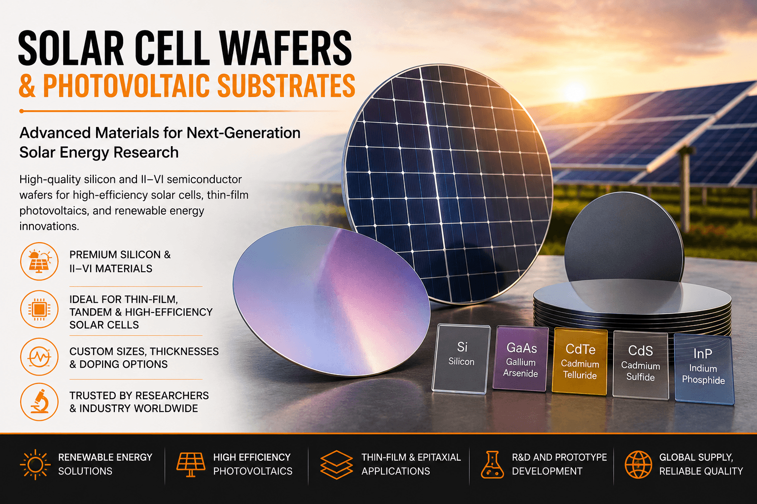
Our portfolio includes monocrystalline silicon, polycrystalline silicon, and advanced compound semiconductor materials such as GaAs, CdTe, CdS, and InP. These materials are widely used to fabricate high-efficiency solar cells, tandem photovoltaic devices, thin-film solar cells, and experimental renewable energy technologies.
Available Specifications
- Monocrystalline and polycrystalline silicon wafers
- GaAs, CdTe, CdS, and InP photovoltaic substrates
- P-type and N-type silicon
- Custom wafer diameters and thicknesses
- <100>, <111>, and <110> crystal orientations
- Single-side and double-side polished wafers
- Prime, test, and research grades
- Prototype through production quantities
Common Applications
- Silicon solar cells
- Thin-film photovoltaic devices
- Tandem solar cells
- Photonics research
- Thin-film deposition
- Renewable energy research
- Semiconductor process development
- University and government laboratory research
Recent Research Inquiry
"We are developing tandem photovoltaic cells and require polished GaAs substrates with controlled crystal orientation for thin-film deposition and high-efficiency solar device fabrication. Can custom substrate specifications be provided?"
Our engineering team can recommend the optimal wafer material, crystal orientation, conductivity type, and substrate finish for your photovoltaic research or commercial solar cell application.
Get Your Solar Cell Wafer Quote FAST! Or Buy Online and Start Researching Today!
What Are Solar Cell Wafers?
Solar cell wafers are semiconductor substrates used to convert sunlight into electrical energy through the photovoltaic effect. They serve as the foundation for photovoltaic devices by providing the crystalline structure on which p-n junctions, anti-reflective coatings, and conductive contacts are fabricated. While monocrystalline and polycrystalline silicon remain the most widely used materials, advanced compound semiconductors such as gallium arsenide (GaAs), cadmium telluride (CdTe), cadmium sulfide (CdS), and indium phosphide (InP) are increasingly used for high-efficiency and specialized solar cell applications.
UniversityWafer supplies solar cell wafers and photovoltaic substrates for renewable energy research, prototype development, and commercial manufacturing. Custom wafer diameters, thicknesses, crystal orientations, conductivity types, and polishing options are available to support virtually any photovoltaic project.
Materials Used in Solar Cells
Different photovoltaic technologies require different substrate materials depending on efficiency targets, manufacturing methods, operating environments, and overall cost.
| Material | Primary Advantage | Typical Applications |
|---|---|---|
| Monocrystalline Silicon | Highest efficiency and excellent electrical performance | Residential and commercial photovoltaic panels |
| Polycrystalline Silicon | Lower manufacturing cost | Large-scale solar power generation |
| Gallium Arsenide (GaAs) | Very high conversion efficiency | Spacecraft, satellites, concentrated photovoltaics |
| Cadmium Telluride (CdTe) | Cost-effective thin-film technology | Commercial thin-film solar modules |
| Cadmium Sulfide (CdS) | Excellent window layer material | Thin-film photovoltaic devices |
Advantages of High-Quality Photovoltaic Substrates
Selecting the proper photovoltaic substrate improves device efficiency, manufacturing yield, and long-term reliability. High-quality wafers provide superior crystal uniformity, excellent surface quality, and consistent electrical characteristics required for advanced solar cell fabrication.
- High crystal quality
- Excellent surface flatness and polish
- Low defect density
- Available in custom wafer sizes
- Multiple conductivity types
- Custom crystal orientations
- Research and production quantities
- Compatible with advanced photovoltaic processing
Applications
Solar cell wafers are used throughout the renewable energy industry as well as university and government research laboratories developing next-generation photovoltaic technologies.
- Silicon photovoltaic cells
- Thin-film solar cells
- Tandem solar cells
- Perovskite-silicon solar cells
- Photonic devices
- Thin-film deposition
- Renewable energy research
- Semiconductor process development
Solar Cell Materials Comparison
| Technology | Strength | Typical Use |
|---|---|---|
| Monocrystalline Silicon | Highest commercial efficiency | Premium residential and commercial panels |
| Polycrystalline Silicon | Lower manufacturing cost | Utility-scale solar farms |
| Thin-Film CdTe | Excellent large-area manufacturing | Commercial solar modules |
| GaAs Multi-Junction | Exceptional efficiency | Space and aerospace power systems |
| Perovskite Tandem | Next-generation high efficiency | Emerging photovoltaic research |