Gallium Arsenide (GaAs) Wafers
Gallium Arsenide (GaAs) wafers are widely used in high-speed electronics, RF and microwave devices, photonics, laser diodes, LEDs, and high-efficiency solar cells. UniversityWafer supplies research and production-grade GaAs substrates in multiple diameters, orientations, doping types, and surface finishes, including epi-ready wafers for advanced semiconductor fabrication.
Get Your Gallium Arsenide (GaAs) Wafer Quote FAST!
UniversityWafer supplies Gallium Arsenide (GaAs) wafers for
research, prototyping, and commercial semiconductor manufacturing. Whether
your project involves RF electronics, optoelectronics, photonics, or
high-speed integrated circuits, our team can help you select the right
GaAs substrate for your application.
Complete the form below with your desired wafer specifications, and one of our
wafer specialists will quickly provide pricing, availability, and technical
recommendations. We offer both standard inventory and custom-manufactured
gallium arsenide substrates.
Recent Research Inquiry
"Our laboratory is developing high-frequency RF devices and requires
semi-insulating GaAs wafers with a (100) orientation,
epi-ready polish, and a thickness of approximately 625 µm.
Can you provide pricing, lead time, and available diameters for research
quantities?"
Available Custom Specifications
- 2", 3", 4", 6", and custom wafer diameters
- (100), (111), and custom crystal orientations
- Semi-insulating, n-type, and p-type GaAs
- Single-side polished (SSP) and double-side polished (DSP)
- Epi-ready surface finishes
- Prime, test, and research grades
- Custom thicknesses and edge profiles
- Prototype and production quantities
Please include your required diameter, orientation, doping type,
surface finish, thickness, quantity, and any additional processing
requirements in the request form. Our engineers will respond with a
custom quote tailored to your project.
Get Your Quote FAST! Or,
Buy Online
and Start Researching Today!
Why Choose Gallium Arsenide Wafers?
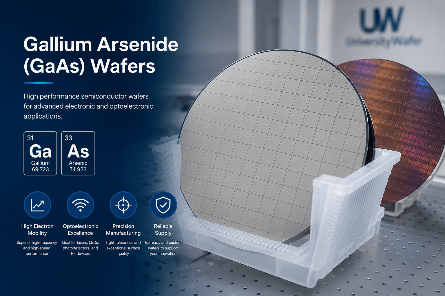
Gallium Arsenide (GaAs) is a high-performance
III-V semiconductor widely used in RF electronics,
optoelectronics, photonics, and high-speed integrated circuits. Compared to
silicon, GaAs provides significantly higher electron mobility and a direct
bandgap, making it ideal for applications requiring fast switching speeds,
high-frequency operation, and efficient light emission.
Advantages of GaAs Substrates
Researchers choose GaAs wafers because they combine excellent
electrical and optical performance with reliable crystal quality. These
substrates are commonly used for epitaxial growth by MBE and MOCVD and are
available in semi-insulating, n-type, and p-type configurations for a variety
of semiconductor devices.
| Property |
Benefit |
| High Electron Mobility |
Supports ultra-fast electronic devices |
| Direct Bandgap |
Excellent for LEDs and laser diodes |
| High Frequency Performance |
Ideal for RF and microwave applications |
| Low Noise Characteristics |
Improves communication system performance |
| Epi-Ready Surfaces Available |
Suitable for advanced epitaxial growth |
Common Applications
- RF integrated circuits (RFICs)
- Microwave and millimeter-wave devices
- 5G communication components
- High Electron Mobility Transistors (HEMTs)
- Heterojunction Bipolar Transistors (HBTs)
- Laser diodes and VCSELs
- Infrared LEDs and photodetectors
- Multi-junction solar cells
- Optical communication systems
- University and semiconductor research
Custom Gallium Arsenide Wafer Specifications
UniversityWafer supplies GaAs substrates in multiple
diameters, orientations, thicknesses, and doping types to support both research
and production. Prime, test, and epi-ready grades are available with
single-side or double-side polished finishes. Custom specifications can be
manufactured to meet the requirements of advanced semiconductor, photonic, and
optoelectronic device fabrication.
Related Resources
