
Request a Quote for Borofloat 33 Glass Wafers
Borofloat® 33 is a premium borosilicate glass developed for demanding optical, semiconductor, and scientific applications. Its exceptional surface quality, high optical transmission, low thermal expansion, and excellent chemical resistance make it an ideal substrate for MEMS devices, microfluidics, anodic bonding, photonics, and precision optics.
UniversityWafer supplies Borofloat 33 wafers in a variety of diameters, thicknesses, and polish options for research laboratories, universities, and commercial manufacturers. Custom wafer specifications are available to meet your application's exact requirements.
Get Your BF33 Wafer Quote FAST! Or, Buy Online and Start Researching Today!
Popular Borofloat 33 Applications
- MEMS fabrication
- Microfluidic devices
- Anodic bonding to silicon
- Optical windows and filters
- Photonics and optoelectronics
- Biosensors and lab-on-a-chip devices
- Semiconductor packaging
- Analytical and biomedical instruments
Need a custom Borofloat 33 wafer? Include your preferred diameter, thickness, edge profile, polish, and quantity in the form above, and our engineering team will recommend the best substrate for your project.
What Are Borofloat 33 Wafer Applications?
Borofloat® 33 is a premium borosilicate glass widely used in semiconductor manufacturing, MEMS fabrication, photonics, optics, biotechnology, and microfluidics. Its exceptional thermal stability, excellent optical transmission, low thermal expansion, and high chemical resistance make it an ideal substrate for demanding research and industrial applications.
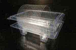 Borofloat 33 wafers are commonly selected when engineers require excellent surface flatness, optical quality, and compatibility with silicon for anodic bonding. These properties have made Borofloat 33 one of the most popular glass substrates for semiconductor packaging, MEMS devices, sensors, and laboratory-on-a-chip technologies.
Common Borofloat 33 Applications
- MEMS devices and microsensors
- Microfluidic chips and lab-on-a-chip devices
- Anodic bonding to silicon wafers
- Optical windows, mirrors, and optical filters
- Photonics and optoelectronic devices
- Biomedical slides, DNA sequencers, and biochips
- Semiconductor packaging and display glass
- Solar collectors and photovoltaic components
- Chemical processing equipment and sight glasses
- High-temperature laboratory equipment
Examples of Borofloat 33 in Research
-
 Glass sensors and optical sensing platforms
-
 Interdigitated electrode arrays used in biosensors and chemical sensing.
-
 MEMS packages for pressure, acceleration, and gyroscope sensors used in automotive, aerospace, and telecommunications industries.
-
 Large-area photon-counting imaging detectors for astronomy, scientific instrumentation, and low-light imaging systems.
Popular Borofloat 33 Wafer Specifications
Order Borofloat 33 Glass Wafers Online
- Diameter: 100 mm (4") ±0.3 mm
- Thickness: 500 ±25 µm
- Optional Thickness: 175 ±25 µm
- Surface Finish: Double Side Polished (DSP)
- Surface Roughness: <1.5 nm Ra
- TTV: <10 µm
- Edge: Ground C-shape with SEMI primary flat
- Scratch/Dig: 60-40 (MIL-PRF-13830)
- Packaging: Class 1000 cleanroom packaged