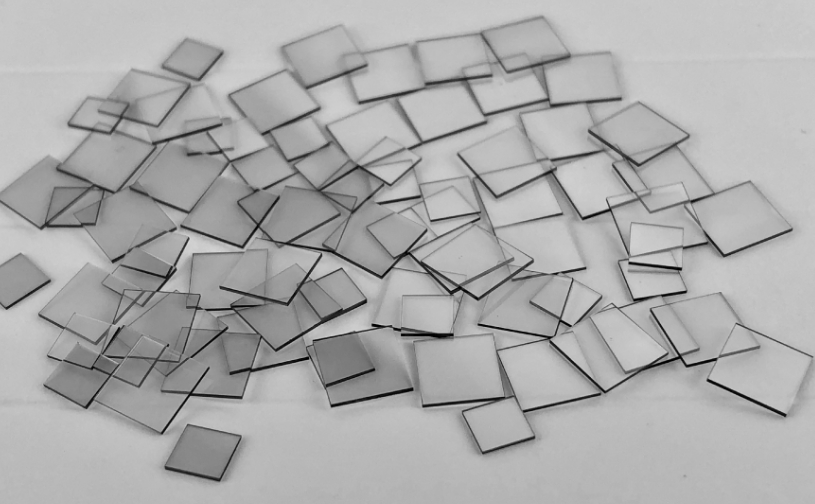
Diamond-Coated Wafers for Advanced Thermal Management in AI and Power Chips
As transistor densities climb and AI accelerators reach unprecedented power levels, heat has become one of the greatest barriers to performance. UniversityWafer offers diamond-coated silicon and SiC wafers that combine exceptional thermal conductivity with electrical insulation, helping researchers and engineers push device limits safely and efficiently.
Cool Smarter, Run Faster
Explore diamond-coated wafers engineered to manage extreme thermal loads in AI and RF chips.
Get Your Quote FAST! Or, Buy Online and Start Researching Today!
Applications
• AI, GPU, and data-center cooling• GaN/SiC RF amplifiers and power electronics
• MEMS and sensor substrates requiring high heat dissipation
• Optical components and quantum research devices
UniversityWafer’s diamond-coated wafers integrate seamlessly into research and production workflows. Thin polycrystalline diamond films can be customized for thickness, grain size, and substrate type—from standard silicon to sapphire and carbide bases.
Performance gains: research has shown temperature reductions of up to 70 °C in GaN HEMTs and significant improvements in power density, reliability, and RF gain. These coatings are poised to redefine thermal limits in AI, 5G, and next-generation computing.
Diamond-Coated Wafers: Turning Hot Spots into Headroom
Today’s AI and high-performance chips pack extreme transistor density and switch at multi-GHz rates. The result is localized hot spots that throttle CPUs/GPUs and shorten lifetime. A new pathway is emerging: integrate a micrometer-thin, polycrystalline diamond film within nanometers of where heat is generated so it can spread laterally and vertically before it concentrates.
Why Diamond?
- Ultra-high thermal conductivity: diamond spreads heat far better than copper or silicon.
- Electrical insulator: acts as a “thermal dielectric” — conducts heat without carrying current.
- Chemical and mechanical robustness: resists wear, corrosion, and high fields; ideal near active devices.
- Thin-film friendly: polycrystalline films (≈0.3–2 µm typical) can blanket devices and interconnects.

Low-Temperature Integration (≈400 °C Class)
Traditional CVD diamond needed >900–1000 °C — incompatible with finished CMOS. New recipes introduce oxygen into the carbon-rich plasma to suppress non-diamond phases, enabling large-grained diamond growth near ~400 °C. That’s low enough to preserve delicate metals and dielectrics in advanced chips.
- Conformal coverage: sidewalls and top surfaces can be coated to surround hot devices.
- Thin by design: films stay micrometer-scale to minimize stress and preserve planarity.
Interface Matters: Beating Thermal Boundary Resistance
Heat transfer can bottleneck at material interfaces (thermal boundary resistance, TBR). During low-temp growth on common caps (e.g., SiNx), intermixing can form a silicon-carbide (SiC) bridge layer that improves phonon coupling into diamond — lowering TBR and boosting real device temperature drops.
Measured Wins in Real Devices
- GaN HEMTs (RF): surround-coat diamond layers have shown 50–70 °C channel temperature reduction, enabling higher RF power and improved gain at X-band frequencies.
- AI/CMOS hot spots: models and prototypes indicate diamond layers above transistors can flatten hot-spot gradients, increasing sustained performance before thermal throttling.
- 3D stacks: when paired with vertical “thermal pillars,” diamond scaffolding provides layer-to-layer heat highways critical for HBM, chiplets, and future multi-tier AI accelerators.
Where Diamond-Coated Wafers Help Most
- AI Accelerators & GPUs: sustain higher clocks under heavy kernels by taming hot spots.
- RF Power (GaN, SiC): power amps and front-ends with lower junction temps and improved reliability.
- Power Conversion: dense DC-DC and motor drives where thermal margins constrain efficiency.
- MEMS & Sensors: hard, stable, chemically resistant passivation with superior heat spreading.
Thermal Conductivity Quick Compare
| Material | Thermal Conductivity (W·m⁻¹·K⁻¹) | Electrical |
|---|---|---|
| Polycrystalline Diamond (thin film) | ~1000–1800* | Insulator |
| Copper | ~400 | Conductor |
| Silicon | ~150 | Semiconductor |
| Silicon Nitride | ~20–30 | Insulator |
*Thin-film poly-diamond varies with grain size, thickness, and interface quality; thick high-quality films can be higher.
UniversityWafer Solutions & Options
- Diamond-Coated Silicon, SiC, Sapphire: substrates tailored for thermal spreading layers and optical windows.
- Film Options: nano- to micro-crystalline CVD diamond; target thickness windows typically 0.3–2 µm.
- Interface Engineering: SiNx/SiC interfacial stacks to reduce TBR into diamond.
- Formats: research quantities to production lots; wafers diced on request.
Glossary
- Thermal Boundary Resistance (TBR): resistance to heat flow at a material interface.
- Thermal Scaffolding: network of diamond spreaders and vertical thermal pillars inside 3D stacks.
- HEMT: High-Electron-Mobility Transistor, common in RF power (e.g., GaN).
- Polycrystalline Diamond: diamond film composed of many grains; ideal as thin-film heat spreader.
Note: Performance depends on device architecture, grain size, thickness, and interface quality. UniversityWafer can help select wafer + coating combinations for your specific thermal goals.
Citation: Adapted from “Diamond Blankets Will Chill Future Chips,” IEEE Spectrum, November 2025. For related reading, see the feature https://spectrum.ieee.org/calibre-vision-ai-chip-design .
