Mechanical Grade Silicon Wafers Used For Electrostatic Chuck
Ready to Optimize Your Wafer Chuck?
Get a Quote for Refinishing or Test Wafers:
Complete the form below for a rapid response, or Buy Online Now to start your research today.
Electrostatic Wafer Chuck
Question
By chance, have you ever measured the dielectric constant of your 300mm P-doped <100> Silicon wafers? I’m thinking of buying some to use for dummy wafers in an electrostatic wafer chuck test.
For thickness .775 mm. No other specs like roughness.
Quantity breakpoint at 5 and 10.
We want to use the p-doped wafers to calibrate our electrostatic chuck which requires us to know the dielectric constant of the wafer, and whether it leans more towards insulator or conductor on the spectrum of dielectrics.
Answer:
To answer your question directly: No, we do not measure the dielectric constant of our standard silicon wafers on a batch-by-batch basis.
This is because the dielectric constant (relative permittivity, $\varepsilon_r$) of silicon is a fundamental material property determined by the crystal structure, rather than a variable manufacturing specification like resistivity, thickness, or flatness (TTV).
Here is the data you likely need for your Electrostatic Chuck (ESC) calculations:
1. The Standard Value
For standard monocrystalline silicon (including P-doped <100>), the accepted dielectric constant is approximately 11.7 (at room temperature and low frequencies).
2. The Role of Doping (P-doped)
While we do not measure the dielectric constant, we do measure and specify Resistivity, which is often the more critical variable for ESC "dummy" wafer testing.
-
Dielectric Constant ($\approx$ 11.7): This remains relatively constant regardless of dopant concentration for standard resistivity ranges.
-
Resistivity (Ohm-cm): P-doping (Boron) makes the wafer semi-conductive. In an electrostatic chuck, the wafer typically acts as a conductive electrode rather than an insulator. The clamping force (whether Coulombic or Johnsen-Rahbek) is heavily influenced by how quickly the charge distributes across the wafer, which is dictated by its resistivity.
3. Recommendation for ESC Testing
If you are running an ESC test, you are likely calculating the clamping force:
Note: In this formula, usually refers to the dielectric layer of the chuck, not the wafer, unless you are modeling the depletion layer capacitance of the silicon itself.
If you need consistent dummy wafers for this application, standard Mechanical Grade 300mm wafers are the industry standard choice because they provide the correct mechanical weight, flex, and conductivity for charge dissipation without the high cost of Prime grade silicon.
Next Step:
You can view our available inventory of 300mm Silicon Wafers
Reference #323755 for specs and pricing.
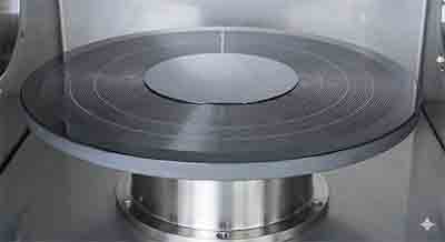
What this image is showing:
This image illustrates a Silicon Wafer (the dark, highly reflective disc in the center) resting on top of an Electrostatic Chuck (ESC) (the larger metallic platform underneath).
-
The Chuck Surface: The visible concentric rings (grooves) on the metallic surface are a key feature of ESCs. These channels are often used for backside gas cooling (typically Helium) to regulate the wafer's temperature during high-energy processes like plasma etching.
-
The Clamping Action: The image visualizes the moment where the electrostatic force (Coulombic or Johnsen-Rahbek) would be activated to clamp the wafer flat against the dielectric surface.
-
The Application: This setup demonstrates exactly where your Mechanical Grade Dummy Wafers are used—to test that clamping force, check for gas leaks in those grooves, and calibrate the tool without risking a Prime wafer.
Electrostatic chucks (ESCs) Importance In Semiconductor Manufacturing
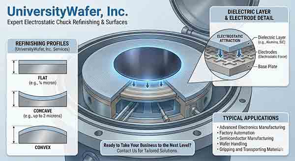
Electrostatic chucks (ESCs) are essential in semiconductor manufacturing for securely holding wafers, and UniversityWafer, Inc. offers expert refinishing services to restore or reshape ESC surfaces—including various dielectric materials and profiles—to precise flatness or curvature specifications, thereby enhancing performance and preventing plasma damage across applications such as electronics manufacturing, wafer handling, and factory automation.

Electrostatic chucks (ESCs) play a vital role in semiconductor manufacturing. They securely hold wafers during various processes, such as etching, deposition, and lithography. ESCs use an electrostatic force to attract the wafer to the chuck’s surface, ensuring stable contact and preventing damage.
Refinishing is necessary because the surfaces of the ESCs degrade over time due to wear, the need for specific surface profiles, or plasma damage. Refinishing ESCs used in plasma etching helps prevent chuck failure caused by plasma damage. It also can fix minor surface imperfections or alter the chuck’s geometry for particular applications.
UniversityWafer, Inc. has been successfully processing ESCs for several decades. UniversityWafer can refinish your chuck to meet specifications, whether flat, concave, or convex, and can lap or polish it to achieve your desired surface finish.
Electrostatic chucks, which usually conform to SEMI standard sizes of 100mm, 125mm, 150mm, 200mm, 300mm, and 450mm in diameter, can have a dielectric layer made from various materials. UniversityWafer supplies and refinishes these critical materials, including:
- Alumina (Al2O3): Available in various forms, such as Sapphire (Item #2562).
- Sapphire: High-durability substrates like Item #4158.
- Silicon Carbide: Including robust options like Item #3912.
- Glass: Specialized wafers such as Item #517.
- Other materials including polyimide, epoxy, Silicon Nitride, SiSiC, and thermal spray.
UniversityWafer can reshape these ESCs or e-chucks to achieve your desired flatness, whether flat, concave, or convex. For example, we can achieve flatness down to ¼ micron, concave to ¼ micron, or from ½ micron to concave at 2 microns, and the same applies to convex chucks. Depending on your application, UniversityWafer can remove as little as ¼ micron of material. Removing minimal material can eliminate defects, flatten, or change the shape to convex or concave, and additional material can also be removed as needed.
Based on our extensive experience, UniversityWafer can lap or polish all these various materials that make up the dielectric layer. In addition to refinishing used chucks, we can also reshape new electrostatic chucks to different levels of flatness or to concave or convex shapes as required. Electrostatic (ESC) chucks may also have grooves, bumps, or other surface features and designs.
Typical Applications of Electrostatic Chucks Include:
- Advanced Electronics Manufacturing
- Electrostatic Bulletin Boards
- Factory Automation
- Gripping and Transporting Materials
- Semiconductor Manufacturing
- Wafer Handling
Ready to Take Your Business to the Next Level?
At UniversityWafer, Inc., we combine innovation, precision, and reliability to deliver top-quality manufacturing solutions tailored to your needs. Whether you’re seeking efficiency, speed, or scalability, we’re here to assist you.

