Explore silicon-on-glass and silicon-on-insulator wafers for patterning nanoscale structures that control light. Specify the operating wavelength, device-layer thickness, substrate, surface finish, and wafer size when requesting a quote.
Silicon-on-Glass for Optical Metasurface Fabrication
I wish to buy a wafer of thin layers of silicon-on-glass, for optical metasurface fabrication. I wonder about several things:
Where exactly in your website can I find this product?
What is the possible thickness of the silicon layer? Can it be customized? I need about a 150 nm thick layer.
A transparent glass support can be useful for transmission-mode optics. A silicon layer near 150 nm may be a starting specification, but the required thickness and nanostructure geometry depend on the operating wavelength and optical design. Confirm glass type, silicon film type, thickness tolerance, and availability when requesting a custom substrate.
Reference #256054 for specs and pricing.
Get Your Optical Metasurface Substrate Quote FAST! Send your target specifications below, or browse available wafers online.
Silicon-on-Insulator for Optical Metasurface Fabrication
A Physics PhD student requested a quote for the following:
Could we order a set of SOI wafers with the following specifications: Device Layer thickness: 1um Device layer resistivity: 10 Ohm.cm (or higher), Phosphorous-doped Box (oxide) thickness: 2um Handle Resistivity: 1000 Ohm.cm (or higher) We can take any wafer size - whatever will have the shortest lead time. Double side polished would be our preference, and we would be willing to pay more for this. However, if you only have single side polished, this also works. We would also be willing to pay more for shorter lead time. Looking forward to hearing back from you.
We are fabricating an optical metasurface, the resonators of which will be 910nm in height (hence the need for 1um device layer).
Could you send over the information about the 2um SOI you mentioned earlier? It may be possible for us to thin it down to 910nm.
Silicon-on-insulator (SOI) wafers have a crystalline silicon device layer above a buried oxide (BOX) and a silicon handle wafer. The device layer can be patterned into resonators; the BOX provides optical index contrast. Unlike glass-backed SOG, a standard SOI handle is silicon, so suitability for through-substrate transmission depends on wavelength and device design. The 1 µm device layer and 910 nm resonator height above are research specifications, not stock availability claims. The quoted phrase “phosphorous-doped BOX” needs clarification: BOX is silicon dioxide, whereas phosphorus doping normally describes the silicon device layer or handle. Confirm the intended layer, BOX thickness, device-layer thickness, resistivity, and finish for your design.
Reference #275099 for specs and pricing.
What Is an Optical Metasurface?
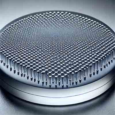
An optical metasurface is a patterned, approximately planar array of nanoscale elements designed to change the phase, amplitude, or polarization of light. The elements, often called meta-atoms, are usually arranged with a subwavelength pitch for the intended operating wavelength. Their response depends on geometry, material, surrounding media, and illumination.
Concept illustration: a patterned dielectric metasurface used as a flat lens. Actual dimensions and performance depend on the optical design.
Choosing a Substrate and Device Layer
manipulate.
Tailored Optical Properties: By designing the shape, size, and arrangement of the meta-atoms, metasurfaces can achieve specific optical functions such as bending, focusing, or filtering light.
Silicon-on-glass combines a silicon device film with a transparent support. SOI provides a crystalline silicon device layer separated from a silicon handle by buried oxide. For other designs, a patterned silicon nitride film on fused silica may be considered; a nitride coating on silicon is not equivalent to nitride on a transparent substrate.
Material choice depends on the wavelength and required transmission. Silicon is useful for many near-infrared designs, while crystalline silicon absorbs strongly across much of the visible spectrum. Transparent dielectric platforms can be preferable for visible-light transmission. Specify the wavelength range before selecting a film and substrate.
Applications and Fabrication
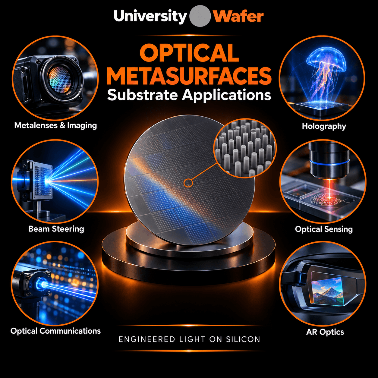
Metalenses: Patterned elements impose a spatially varying optical phase to focus light in a thin form factor.
Beam steering and holography: Arrays can shape the direction or wavefront of incident light.
Polarization and spectral control: Geometry and material can be tailored for polarization-dependent response or filtering.
Typical fabrication uses lithography or other nanoscale patterning followed by etching or deposition. Feature size, sidewall quality, film thickness, and surface roughness can affect optical efficiency. Bandwidth, field of view, and large-area uniformity are additional design constraints. A metalens does not automatically outperform a conventional lens in every application.

 manipulate.