
Most Popular Silicon Wafer Specs for Microelectronics
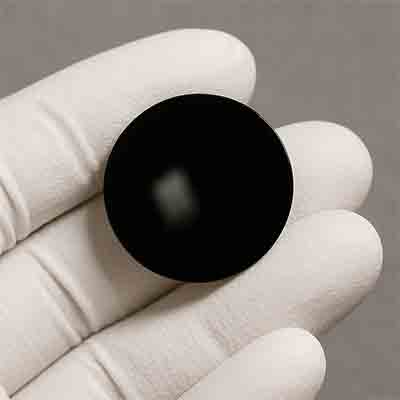
Silicon wafers are the foundation for modern electronic devices, from smartphones and computers to medical equipment and cars. These thin, disc-shaped slices of semiconductor material are used to make integrated circuits and microelectronic components. Choosing the right silicon wafer type is important for device performance, manufacturing success, and cost-effectiveness. Understanding the differences between silicon wafer types helps researchers, engineers, and manufacturers make better choices.
Silicon has become the main material for electronics because it's common in nature, stable, and has electrical properties that can be precisely controlled. Silicon wafers can be customized through different manufacturing methods and doping processes to meet specific needs, making them useful for many types of electronic devices. As technology advances, the need for specialized silicon wafer types continues to grow.
Get Your Quote FAST! Buy Online and Start Researching Today!
Silicon Wafer Variations
In this guide, we'll look at the most popular silicon wafer types used in microelectronics, their characteristics, how they're made, and what they're used for. This information will help you choose which type of silicon wafer is best for your needs.
| Key Takeaways: Silicon Wafer Variations | |
|---|---|
| Wafer Sizes: Silicon wafers range from 1-inch (25.4mm) for research to 300mm (12-inch) for high-volume manufacturing, with each size offering specific advantages for different applications. | Manufacturing Methods: Czochralski (CZ) process creates standard wafers for most applications, while Float Zone (FZ) produces ultra-high purity silicon for specialized devices. |
| Dopant Types: N-type (phosphorus, arsenic) and P-type (boron, gallium) dopants create different electrical properties suited for specific device requirements. | Crystal Orientation: (100), (111), and (110) orientations offer different surface properties affecting oxide growth, etching behavior, and carrier mobility. |
| Surface Treatments: Thermal oxides, silicon nitride coatings, and metallization layers modify wafer surfaces for specific device requirements. | Application Specificity: Wafer selection should be based on specific application needs, balancing performance requirements with cost considerations. |
Silicon Wafer Sizes and Their Applications
The size of a silicon wafer affects what it can be used for and how efficiently it can be manufactured. The semiconductor industry has created standard wafer sizes, each with benefits for different uses. Wafer sizes have grown over time as the industry tries to improve efficiency and lower costs while meeting the needs of more complex electronic devices.
Silicon wafer sizes have increased from 1-inch (25.4mm) wafers in the 1960s to today's standard 300mm (12-inch) wafers used in large-scale manufacturing. Each size increase lets manufacturers make more chips per wafer, lowering the cost per chip and improving production efficiency. This growth has been driven by economics, as larger wafers greatly reduce manufacturing costs when producing at scale. Different wafer sizes still have important roles in various parts of the microelectronics industry, from cutting-edge commercial production to specialized research.
1-inch (25.4mm) Silicon Wafers
1-inch silicon wafers are among the smallest standard sizes in the industry. These compact wafers are valuable for research and small-scale experiments where saving material is important. Despite their small size, they play a key role in certain parts of the microelectronics world, providing a platform for early-stage development and specialized research.
1-inch silicon wafers have several advantages for specialized uses and education. These small wafers are economical for early research and academic settings where students learn semiconductor basics without the expense of larger wafers. Their reduced size makes them ideal for applications needing only a few devices rather than mass production. They also fit well in specialized testing equipment with limited sample space, letting researchers do preliminary experiments before moving to larger wafer sizes.
- Ideal for university research laboratories and educational institutions
- Cost-effective for small-scale device fabrication and testing
- Perfect for specialized applications with limited space requirements
- Available in various crystal orientations and dopant types
- Compatible with smaller research equipment that cannot accommodate larger wafers
4-inch (100mm) Silicon Wafers
4-inch or 100mm silicon wafers are one of the most versatile and widely used sizes in both research and industry. These medium-sized wafers balance usable area and cost, making them popular across many sectors of the microelectronics industry. They've become a standard for many fabrication processes, especially in research and specialized production facilities where the economics of larger wafers may not make sense.
4-inch silicon wafers hit a sweet spot between research usefulness and commercial viability. They provide enough area for complex circuit designs while remaining easy to handle and process. This balance makes them valuable for university research labs, small-scale production facilities, and specialized device manufacturing. The 100mm format allows for reasonable device yields without needing the sophisticated automation and handling systems required for larger wafer sizes, making them accessible to more users and facilities with moderate equipment investments.
100mm silicon wafers are particularly valuable for applications requiring specialized processing or custom specifications. They are commonly used in the development of MEMS devices, sensors, and other specialized electronic components where the higher costs of larger wafers would be prohibitive. Their widespread adoption also means that processing equipment for this size remains readily available, making them accessible for a wide range of users.
5-inch (125mm) Silicon Wafers
5-inch or 125mm silicon wafers hold an interesting position in the semiconductor industry. These wafers are a transitional size between the widely used 4-inch (100mm) wafers and the larger 6-inch (150mm) wafers. While less common than 4-inch and 6-inch wafers, 125mm wafers have important roles in specific applications and manufacturing scenarios, particularly in specialized industrial sectors and certain regions where this size became standard for historical reasons.
5-inch silicon wafers provide a middle ground that balances increased usable area with manageable handling requirements. These wafers are particularly valuable for certain applications where 4-inch wafers would be too small but 6-inch wafers would be excessive. This makes them an efficient choice for specialized manufacturing needs and certain research applications.
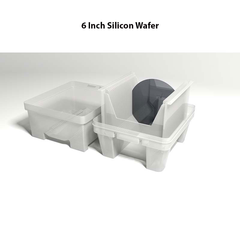
6-inch (150mm) Silicon Wafers
6-inch or 150mm silicon wafers represent a significant step toward high-volume production capability while remaining reasonably easy to handle. These wafers have become a standard in many production environments because they balance yield and cost. They're widely used for certain applications and device types, particularly for analog circuits, power devices, and specialized components that don't require the advanced processes typically used with larger wafer sizes.
6-inch silicon wafers offer substantial manufacturing advantages compared to smaller wafer sizes. They provide significantly more die per wafer than 4-inch or 5-inch alternatives, improving economics for medium to high-volume production. At the same time, they remain manageable for handling and processing without requiring the extensive automation systems needed for larger wafer sizes.
Manufacturing Processes and Silicon Wafer Types
The manufacturing process used to create silicon wafers significantly impacts their properties and suitability for specific applications. Different crystal growth methods result in wafers with distinct characteristics that make them appropriate for various microelectronic purposes. Understanding these processes helps in selecting the optimal wafer type for a given application.
Silicon wafer manufacturing involves complex processes that determine the material's purity, crystal structure, and electrical properties. The choice between different manufacturing methods depends on the intended application's requirements and the desired balance between cost and performance characteristics. Each method has tradeoffs in terms of purity, defect density, scalability, and production economics that determine which wafer type is most suitable for specific device requirements.

Czochralski (CZ) Silicon Wafers
The Czochralski process is the most common method for silicon crystal growth in the semiconductor industry. This technique produces high-quality single-crystal silicon ingots that form the basis for most commercial silicon wafers. Named after Polish scientist Jan Czochralski who discovered the method in 1916, this process has become the backbone of silicon wafer production worldwide, accounting for approximately 80-90% of all silicon wafers manufactured for semiconductor applications.
Czochralski silicon wafers offer an excellent combination of quality, consistency, and cost-effectiveness that makes them suitable for a wide range of applications. The controlled manufacturing process creates wafers with well-defined properties and predictable behavior, essential for reliable semiconductor device fabrication.
Float Zone (FZ) Silicon Wafers
Float Zone silicon represents a premium alternative to CZ material, offering exceptionally high purity for specialized applications. This manufacturing method creates wafers with minimal oxygen content and other impurities, making it ideal for devices where absolute material purity is critical. While more expensive than CZ silicon, FZ wafers provide superior electrical properties that are essential for certain high-performance applications where the presence of oxygen or other impurities would significantly degrade device performance or reliability.
Float Zone silicon wafers are manufactured through a process that avoids contact between the molten silicon and any container. Instead, a vertical polysilicon rod is partially melted using radio frequency heating, and a narrow molten zone is moved along the length of the rod. As this molten zone "floats" through the material, it carries impurities with it, resulting in extremely pure silicon crystal formation.
- Produces ultra-high purity silicon with minimal oxygen and carbon contamination
- Ideal for high-performance devices where impurities would degrade performance
- Particularly valuable for power electronics and high-voltage applications
- Essential for certain research applications requiring pristine semiconductor material
- Offers superior electrical properties for specialized detector and sensor applications
Multi-crystalline Silicon Wafers
Multi-crystalline silicon wafers offer a cost-effective alternative to single-crystal materials for applications where absolute crystalline perfection is less critical. These wafers contain multiple crystal grains rather than a single continuous crystal structure, resulting in different electrical and mechanical properties compared to their single-crystal counterparts. The presence of grain boundaries creates distinct characteristics that can be either advantageous or detrimental depending on the specific application requirements.
The production of multi-crystalline silicon typically involves casting molten silicon into molds where it solidifies into blocks with multiple crystal orientations. This process is simpler and less energy-intensive than the methods used to create single-crystal silicon, resulting in significantly lower manufacturing costs.
Dopant Variations and Electrical Properties
The electrical properties of silicon wafers are primarily determined by the type and concentration of dopants introduced during manufacturing. Dopants are carefully selected impurities that alter silicon's semiconductor characteristics, enabling the creation of various device types and functionality. The control of dopant type and concentration represents one of the most powerful tools for customizing silicon wafers for specific applications.
Dopant selection fundamentally changes how silicon behaves in electronic circuits. By introducing elements from either group III or group V of the periodic table, manufacturers can create p-type or n-type semiconductors with distinct electrical behaviors. This controlled modification of silicon's properties forms the foundation of modern semiconductor devices, from the simplest diodes to the most complex integrated circuits.
Undoped (Intrinsic) Silicon
Undoped or intrinsic silicon wafers contain extremely low levels of impurities, maintaining silicon's natural semiconductor properties without intentional modification. These high-purity wafers serve specific purposes in the microelectronics ecosystem where the natural characteristics of silicon are desired. While less common than doped alternatives, intrinsic silicon plays an important role in certain specialized applications where minimal carrier concentration and high resistivity are essential performance requirements.
Pure silicon has a balanced number of electrons and holes, resulting in very low electrical conductivity at room temperature. This intrinsic semiconductor behavior makes undoped silicon valuable for applications requiring minimal background carrier concentration. The high resistivity of intrinsic silicon creates distinct electrical characteristics that are advantageous for specific device types and research purposes.
N-type Silicon Wafers
N-type silicon wafers are doped with elements like phosphorus, arsenic, or antimony to create an excess of negative charge carriers (electrons). These wafers have distinct electrical characteristics that make them suitable for specific device types and applications. The "n" in n-type stands for "negative," referring to the negative charge of the electrons that serve as the majority carriers in this material.
The doping process for n-type silicon involves introducing atoms from group V of the periodic table, which have five valence electrons, into the silicon crystal lattice. Since silicon atoms have four valence electrons, the extra electron from each dopant atom becomes free to move through the crystal, increasing the material's conductivity.
P-type Silicon Wafers
P-type silicon wafers contain dopants such as boron, gallium, or indium that create a deficiency of electrons, resulting in positive charge carriers (holes). These wafers exhibit characteristics that complement n-type materials in semiconductor device design. The "p" in p-type stands for "positive," referring to the positive charge of the holes that serve as the majority carriers in this material.
The doping process for p-type silicon involves introducing atoms from group III of the periodic table, which have three valence electrons, into the silicon crystal lattice. Since silicon atoms have four valence electrons, each dopant atom creates a "hole" or absence of an electron in the crystal structure. These holes can move through the material and function as positive charge carriers, giving p-type silicon its distinctive electrical properties.
Surface Treatments and Specialized Coatings
Surface treatments and specialized coatings significantly enhance silicon wafer functionality for specific applications. These modifications alter the wafer's surface properties without changing the bulk material characteristics, enabling customization for various microelectronic requirements. The ability to modify surface properties expands the versatility of silicon wafers and allows them to be optimized for different device types and manufacturing processes.
The surface of a silicon wafer plays a crucial role in device performance and manufacturing yield. Various treatments can modify properties such as electrical behavior, chemical reactivity, and mechanical durability. These modifications expand the versatility of silicon wafers across different application domains, from integrated circuits to sensors and specialized electronic components.
Thermal Oxide Layers
Thermal oxide layers represent one of the most common and important surface modifications applied to silicon wafers. These silicon dioxide (SiO₂) layers serve multiple critical functions in semiconductor device fabrication, from electrical insulation to surface passivation. The ability to grow high-quality oxide layers with precisely controlled thickness is a fundamental capability in silicon wafer processing.
Thermal oxidation occurs when silicon wafers are exposed to oxygen or water vapor at elevated temperatures, typically between 900°C and 1200°C. The resulting oxide grows into the silicon surface while also building up above it, creating a high-quality dielectric layer that's integral to modern semiconductor devices.
Silicon Nitride Coatings
Silicon nitride (Si₃N₄) coatings provide alternative surface properties compared to silicon dioxide, offering advantages for specific applications and processing requirements. These coatings are typically deposited rather than grown from the substrate, allowing them to be applied to various materials beyond silicon. The distinct properties of silicon nitride make it valuable for applications ranging from advanced semiconductor devices to solar cells and MEMS structures.
Silicon nitride coatings are typically applied using chemical vapor deposition (CVD) techniques, creating uniform layers with precisely controlled thickness and composition. The material's distinct properties make it valuable for applications ranging from advanced semiconductor devices to solar cells and MEMS structures. Its excellent barrier properties and mechanical durability make it particularly useful for protecting underlying structures during subsequent processing steps.
Crystal Orientation and Silicon Wafer Properties
The crystal orientation of silicon wafers significantly affects their properties and suitability for different applications. Silicon crystals can be cut along different crystallographic planes, each offering distinct characteristics in terms of surface properties, etching behavior, and electronic performance. Understanding these orientations is crucial for selecting the optimal wafer type for specific device requirements and manufacturing processes.
Crystal orientation is defined by Miller indices that describe the specific crystallographic plane exposed at the wafer surface. The three most common orientations are (100), (111), and (110), each offering unique advantages for different applications. The choice of crystal orientation affects fundamental properties such as carrier mobility, surface reactivity, and mechanical strength, making it an important consideration in wafer selection.
(100) Silicon Wafers
(100) orientation silicon wafers are the most commonly used wafers in the semiconductor industry, accounting for the vast majority of commercial integrated circuit manufacturing. This orientation offers optimal properties for modern CMOS devices and provides the best combination of electrical performance and manufacturing compatibility. The (100) surface structure creates ideal conditions for growing high-quality oxide layers and achieving excellent interface properties essential for modern semiconductor devices.
The popularity of (100) silicon wafers stems from their superior electrical characteristics and compatibility with standard semiconductor processing techniques. The atomic arrangement at the (100) surface provides the lowest interface state density when silicon dioxide is grown thermally, resulting in better electrical performance for MOSFETs and other critical devices. This orientation also offers excellent uniformity across the wafer surface, contributing to higher manufacturing yields and more consistent device performance.
(111) Silicon Wafers
(111) orientation silicon wafers offer distinct properties that make them valuable for specific applications, particularly in areas where mechanical strength and certain etching characteristics are important. While less common than (100) wafers for integrated circuits, (111) wafers have important roles in specialized applications including MEMS devices, certain types of sensors, and research applications where the unique properties of this orientation provide advantages.
The (111) crystal orientation provides the highest atomic packing density and strongest mechanical properties among the common silicon orientations. This makes (111) wafers particularly valuable for applications requiring mechanical robustness or specific etching behaviors. The orientation also offers unique surface chemistry properties that can be advantageous for certain types of device structures and specialized processing techniques.
(110) Silicon Wafers
(110) orientation silicon wafers represent a specialized option with unique properties that make them valuable for specific research and development applications. While less commonly used than (100) or (111) orientations, (110) wafers offer distinct characteristics that can be advantageous for certain device types and research purposes. The orientation provides unique surface properties and carrier mobility characteristics that are valuable in specialized applications.
The (110) crystal orientation offers intermediate properties between (100) and (111) orientations, providing a compromise between different characteristics. This orientation can be particularly valuable for research applications where the specific surface properties or carrier transport characteristics of (110) silicon provide advantages for device development or fundamental studies of semiconductor behavior.
Specialized Silicon Wafer Applications
Silicon wafers serve diverse applications beyond traditional integrated circuits, each requiring specific characteristics and modifications. These specialized applications often demand customized wafer properties, from surface treatments to specific dopant profiles, enabling the development of devices that push the boundaries of technology. Understanding these applications helps in appreciating the full scope of silicon wafer variations and their importance in modern technology.
The versatility of silicon as a semiconductor material has led to its adoption in numerous specialized fields, each with unique requirements that drive the development of specific wafer types. From high-power electronics to biomedical sensors, these applications demonstrate the adaptability of silicon technology and the importance of having diverse wafer options available to meet specific performance requirements.
Power Electronics and High-Voltage Applications
Power electronics represent one of the most demanding applications for silicon wafers, requiring materials that can handle high voltages, large currents, and elevated temperatures while maintaining reliability and efficiency. These applications often require specialized wafer types with specific dopant profiles, crystal orientations, and surface treatments to achieve optimal performance. The growing importance of power electronics in renewable energy systems, electric vehicles, and industrial automation continues to drive innovation in specialized silicon wafer technologies.
High-voltage applications place unique demands on silicon wafers, requiring careful control of material properties to achieve reliable breakdown voltages and minimize leakage currents. Float Zone silicon wafers are often preferred for these applications due to their superior purity and reduced defect density, which directly impact device reliability and performance under extreme electrical stress conditions.
MEMS and Sensor Applications
Microelectromechanical Systems (MEMS) and sensor applications require silicon wafers with specific mechanical and electrical properties to enable the creation of devices that combine electronic and mechanical functionality. These applications often require precise control of crystal orientation, surface treatments, and wafer thickness to achieve optimal performance. The ability to etch silicon anisotropically and create complex three-dimensional structures makes certain wafer orientations particularly valuable for MEMS applications.
Sensor applications often require specialized surface treatments or coatings to achieve desired sensitivity, selectivity, and stability characteristics. Silicon wafers for these applications may include specific oxide layers, metal coatings, or other surface modifications that enable interaction with the environment while maintaining electrical functionality.
Photovoltaic and Solar Cell Applications
Solar cell applications represent a significant market for specialized silicon wafers, requiring materials optimized for light absorption, carrier collection, and long-term reliability under outdoor conditions. These applications often use different wafer types compared to integrated circuits, with multi-crystalline silicon being common for cost-sensitive applications while single-crystal wafers are used for high-efficiency devices.
Photovoltaic applications require careful optimization of wafer properties including thickness, surface texturing, and dopant profiles to maximize light absorption and carrier collection efficiency. Surface treatments such as anti-reflection coatings and passivation layers are crucial for achieving optimal solar cell performance and long-term reliability.
Quality Control and Wafer Characterization
Quality control represents a critical aspect of silicon wafer manufacturing, ensuring that each wafer meets the precise specifications required for successful device fabrication. Advanced characterization techniques are employed throughout the manufacturing process to monitor and control wafer properties, from crystal structure and dopant distribution to surface quality and contamination levels. These quality control measures are essential for achieving the high yields and reliable performance expected in modern semiconductor manufacturing.
Modern silicon wafer characterization involves sophisticated analytical techniques that can detect and quantify minute variations in material properties. These measurements provide the detailed information necessary to optimize manufacturing processes and ensure consistent wafer quality across production lots. The ability to precisely characterize wafer properties enables continuous improvement in manufacturing processes and helps identify potential issues before they affect device performance.
Electrical Characterization
Electrical characterization of silicon wafers involves measuring properties such as resistivity, carrier concentration, and mobility to ensure that electrical specifications are met. These measurements are typically performed using techniques such as four-point probe resistivity mapping, Hall effect measurements, and capacitance-voltage profiling. The data obtained from these measurements provides critical feedback for process control and quality assurance.
Advanced electrical characterization techniques can detect subtle variations in electrical properties across a wafer surface, enabling identification of process-related issues and optimization of manufacturing parameters. These measurements are essential for ensuring that wafers meet the precise electrical specifications required for successful device fabrication.
Physical and Structural Analysis
Physical and structural analysis of silicon wafers encompasses measurements of crystal structure, surface morphology, and defect density. Techniques such as X-ray diffraction, atomic force microscopy, and transmission electron microscopy provide detailed information about wafer structure and quality. These analyses are crucial for understanding how manufacturing processes affect wafer properties and for optimizing production parameters.
Surface quality analysis is particularly important for silicon wafers, as surface defects can significantly impact device performance and manufacturing yield. Advanced microscopy techniques can detect and characterize surface features at the nanometer scale, providing the detailed information necessary for process optimization and quality control.
Future Trends in Silicon Wafer Technology
The future of silicon wafer technology continues to evolve in response to advancing semiconductor device requirements and emerging applications. Ongoing developments include larger wafer sizes, improved material purity, advanced surface treatments, and specialized wafer types for emerging technologies. These trends reflect the continuous push for better performance, higher efficiency, and lower costs in semiconductor manufacturing.
Emerging applications in areas such as artificial intelligence, quantum computing, and advanced sensors are driving demand for specialized silicon wafer types with unique properties. These developments require continued innovation in crystal growth techniques, surface treatments, and characterization methods to meet the demanding requirements of next-generation devices.
Advanced Manufacturing Techniques
Advanced manufacturing techniques are being developed to produce silicon wafers with enhanced properties and reduced costs. These include improved crystal growth methods, advanced doping techniques, and innovative surface treatment processes. The goal is to produce wafers that meet the increasingly stringent requirements of modern semiconductor devices while maintaining economic viability for large-scale production.
Automation and process control improvements are also playing important roles in advancing silicon wafer manufacturing, enabling better consistency, higher yields, and reduced costs. These technological advances help ensure that silicon wafer technology continues to meet the evolving needs of the semiconductor industry.
Conclusion
Silicon wafer variations represent a rich and diverse technology landscape that enables the creation of virtually all modern electronic devices. From the smallest research wafers to large-scale production substrates, from ultra-pure Float Zone material to cost-effective multi-crystalline alternatives, the variety of available silicon wafer types ensures that optimal solutions exist for virtually any microelectronic application.
Understanding the characteristics and applications of different silicon wafer types is essential for making informed decisions in semiconductor device development and manufacturing. The choice of wafer size, crystal growth method, dopant type, crystal orientation, and surface treatments all significantly impact device performance, manufacturing yield, and cost-effectiveness. By carefully considering these factors, engineers and researchers can select the optimal wafer type for their specific applications.
As technology continues to advance, the demand for specialized silicon wafer types will likely continue to grow, driving further innovation in crystal growth techniques, surface treatments, and characterization methods. The ongoing evolution of silicon wafer technology ensures that this fundamental material will continue to enable breakthrough advances in electronics, computing, renewable energy, and countless other applications that define modern life.
The semiconductor industry's continued reliance on silicon wafers, combined with ongoing technological advances, ensures that understanding these variations remains crucial for anyone involved in electronic device development, manufacturing, or research. Whether selecting wafers for cutting-edge research or high-volume production, the principles and considerations outlined in this guide provide a foundation for making informed decisions that optimize performance, yield, and cost-effectiveness in microelectronic applications.