
"Is it possible to order this item but without the primary flat (simple round substrate)? Maintaining all other specs would be preferred, but we can discuss tradeoffs if necessary. Side note – looking forward, looking for same thickness and TTV at the 200mm OD size as well, but focus today is on the above request."
Primary Orientation Flat on Silicon Wafers
The primary orientation flat, also known as the major flat, is the longest flat edge machined onto a silicon wafer. It serves as a reference that identifies the wafer's crystallographic orientation, allowing engineers and automated semiconductor equipment to properly align the wafer during manufacturing and research processes.
Before orientation notches became the industry standard for larger diameter wafers, primary and secondary flats were widely used to distinguish crystal orientation and dopant type. Today, primary flats remain common on many research-grade and specialty silicon wafers where precise crystal alignment is critical.
Why Are Primary Flats Important?
The location of the primary flat helps ensure accurate wafer alignment during numerous semiconductor fabrication processes, including:
- Photolithography
- Anisotropic wet etching (KOH and TMAH)
- MEMS fabrication
- Silicon epitaxy
- Wafer bonding
- Deep Reactive Ion Etching (DRIE)
- CMOS and integrated circuit manufacturing
UniversityWafer, Inc. supplies prime, test, mechanical, reclaimed, and custom silicon wafers with standard primary flats, custom flat configurations, orientation notches, or completely round wafers depending on your research or production requirements.
Get Your Custom Silicon Wafer Quote FAST! Or, Buy Online and start your research today!
Learn More About Silicon Wafer Flats
Can You Order Silicon Wafers Without a Primary Flat?
Yes. Although most silicon wafers include a primary orientation flat or notch to identify the crystal orientation, many research and specialty applications require completely round wafers without a primary flat. UniversityWafer, Inc. can supply custom silicon wafers manufactured without orientation flats while maintaining your required diameter, thickness, TTV, polish, orientation, resistivity, and other critical specifications.
A corporate scientist asked the following:
The answer is yes. Custom round silicon wafers can often be manufactured without a primary flat while preserving tight dimensional tolerances. Reference #273041 for specifications and pricing.
Why Is the Primary Flat Longer Than the Secondary Flat?
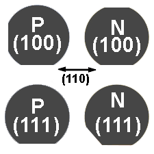
The primary flat, also called the major flat, is intentionally longer than the secondary flat because it serves as the primary reference for identifying the wafer's crystallographic orientation. The secondary flat provides additional information, such as the wafer's dopant type and crystal orientation, depending on SEMI standards.
Before the widespread adoption of orientation notches on larger wafers, flats provided a quick visual method for operators and automated equipment to properly align wafers during semiconductor processing. The longer primary flat minimizes orientation errors and improves repeatability during lithography, oxidation, ion implantation, and wafer handling.
What Is the Purpose of a Primary Flat?
The primary flat identifies the precise crystallographic orientation of a silicon wafer. This orientation determines how silicon behaves during anisotropic etching, oxidation, epitaxial growth, MEMS fabrication, and many other semiconductor manufacturing processes.
Because silicon's crystal structure changes its mechanical, electrical, and chemical properties depending on orientation, correctly identifying the wafer surface is essential for obtaining consistent device performance.
Primary flats are commonly found on:
- <100> silicon wafers
- <111> silicon wafers
- P-type and N-type silicon wafers
- Prime grade silicon wafers
- DSP, SSP, and test-grade wafers
Applications That Depend on Wafer Orientation
Knowing the primary flat location allows researchers and manufacturers to correctly align masks, crystal planes, and process equipment throughout fabrication. Silicon wafer orientation is especially important for:
- MEMS fabrication
- Photolithography
- Anisotropic KOH and TMAH wet etching
- Deep Reactive Ion Etching (DRIE)
- Silicon epitaxy
- Wafer bonding
- Power semiconductor manufacturing
- CMOS and integrated circuit fabrication
- Microfluidic device fabrication
- Semiconductor research and development
Can Primary Flats Be Customized?
Yes. Depending on the wafer diameter and manufacturing process, silicon wafers can often be supplied with custom primary flats, custom secondary flats, orientation notches, or no flats at all. Researchers frequently request custom flats when working with specialized equipment, unique alignment requirements, or non-standard semiconductor processes.
UniversityWafer, Inc. supplies custom silicon wafers in diameters from small research samples through 300 mm production wafers, including prime, test, reclaim, and engineering grades.
Request Custom Silicon Wafer Flats
If your project requires a specific primary flat length, secondary flat configuration, orientation notch, or completely round silicon wafer, our engineering team can recommend the best solution for your application. Contact UniversityWafer with your required diameter, crystal orientation, resistivity, thickness, polish, and quantity for a fast quotation.