
What Is Thermal Oxidation of Silicon?
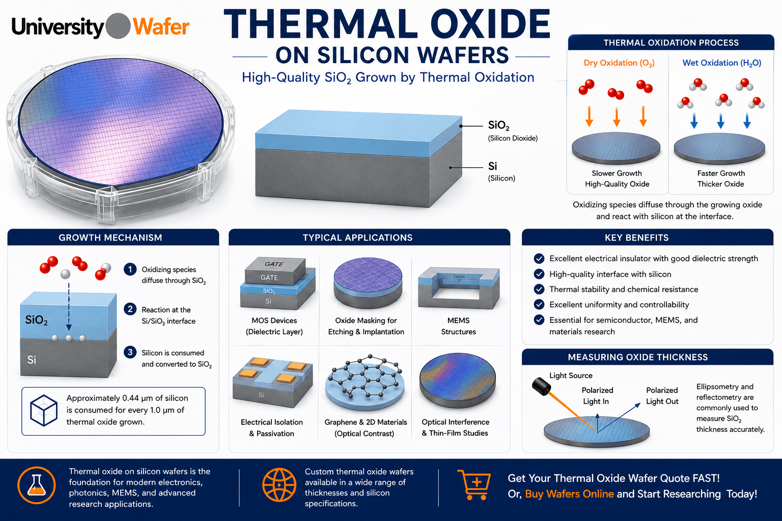
Thermal oxidation of silicon is a high-temperature process used to grow a silicon dioxide (SiO2) layer directly from the surface of a silicon wafer. Unlike a deposited oxide film, thermal oxide forms when an oxidizing species reaches the silicon surface and reacts with silicon atoms.
Thermal oxidation is important in semiconductor processing because properly grown SiO2 can provide excellent electrical insulation and a high-quality interface with crystalline silicon. Thermal oxide is used in semiconductor devices, MOS structures, masking processes, surface passivation, MEMS, and other microfabrication applications.
How Is Thermal SiO2 Grown?
During oxidation, silicon wafers are heated in a furnace or other controlled oxidation system while exposed to an oxidizing ambient. The two principal processes are dry oxidation, which uses molecular oxygen (O2), and wet oxidation, which uses water vapor (H2O) as the oxidizing species.
The overall reactions can be represented approximately as:
Dry oxidation:
Si + O2 → SiO2
Wet oxidation:
Si + 2H2O → SiO2 + 2H2
As oxidation proceeds, oxidizing species must diffuse through the existing oxide to reach the Si/SiO2 interface, where additional silicon is converted into oxide. Consequently, the oxide grows both into the original silicon and outward from the original wafer surface.
Dry Oxidation of Silicon
Dry thermal oxidation uses oxygen as the oxidizing species. It generally produces SiO2 more slowly than wet oxidation under comparable conditions, but it is commonly selected when precise control of relatively thin oxide layers and high electrical quality are important.
Dry oxide has historically been important for high-quality dielectric interfaces in MOS structures. The exact electrical quality of a thermal oxide, however, also depends on substrate preparation, contamination, oxidation conditions, post-oxidation processing, and defect density rather than simply whether the process is classified as dry or wet.
Wet Oxidation of Silicon
Wet thermal oxidation exposes heated silicon to water vapor. Water-related oxidizing species are transported through SiO2 more effectively than molecular oxygen under typical oxidation conditions, so wet oxidation generally produces substantially faster oxide growth.
This makes wet oxidation useful when relatively thick SiO2 layers are required. Depending on the process, thick thermal oxide can be used for electrical isolation, masking, MEMS structures, and other semiconductor fabrication requirements.
Dry Oxide vs. Wet Oxide
The appropriate oxidation method depends on the desired oxide thickness, growth rate, interface requirements, electrical characteristics, and available thermal budget. Neither process is universally better for every application.
- Dry oxidation: slower growth and commonly used when relatively thin, precisely controlled, high-quality oxide is required.
- Wet oxidation: faster growth and commonly used when thicker oxide layers are required.
Researchers selecting thermal oxide silicon wafers should therefore specify both the required SiO2 thickness and other relevant wafer properties rather than selecting an oxidation method based only on growth speed.
Thermal Oxide Growth Rate
The thermal oxide growth rate is influenced by oxidation temperature, oxidizing ambient, pressure, crystallographic orientation, existing oxide thickness, and other process conditions. Oxidation does not normally continue at a constant linear rate as the oxide becomes thicker.
A widely used description of silicon oxidation kinetics is the Deal-Grove model. In this model, thin-oxide growth can have a strong contribution from the reaction occurring at the Si/SiO2 interface, while growth of thicker oxide increasingly becomes limited by transport of oxidizing species through the existing SiO2.
The Deal-Grove model is extremely useful for conventional thermal oxidation, although very thin oxides can show behavior that differs from the simplest form of the model.
Silicon Consumption During Oxidation
Thermal SiO2 is formed by consuming silicon from the substrate. Because the resulting oxide occupies a larger volume than the silicon that reacted, the final oxide extends above and below the location of the original silicon surface.
As a useful approximation, growing a thermal oxide of thickness tox consumes about 0.44 × tox of silicon. The remaining oxide thickness extends outward from the original surface. This dimensional change can be important when designing precision microfabrication and MEMS structures.
Thermal Oxide Thickness
Thermal oxide thickness can range from very thin dielectric films to substantially thicker oxide layers, depending on the oxidation process and application. Required thickness should be selected according to electrical, optical, mechanical, masking, or device requirements.
Oxide thickness can be characterized using techniques such as ellipsometry, reflectometry, or other optical and physical measurement methods. Accurate thickness and uniformity measurements are particularly important when SiO2 forms part of a dielectric stack or optical structure.
The Silicon-Silicon Dioxide Interface
One of the major technological advantages of silicon is its ability to form a stable native compound, SiO2, with an electrically useful Si/SiO2 interface when properly processed. This property played a central role in the development of silicon MOS technology.
Interface traps, fixed oxide charge, contamination, structural defects, and processing history can influence the electrical behavior of the Si/SiO2 system. For electronic applications, careful wafer cleaning and controlled oxidation conditions are therefore essential.
Starting Silicon Wafer Specifications
The properties of the starting semiconductor wafer can influence both thermal processing and subsequent device fabrication. Specifications can include crystal orientation, conductivity type, resistivity, dopant, wafer diameter, thickness, surface finish, and cleanliness.
Common silicon orientations such as <100> and <111> exhibit somewhat different oxidation behavior because surface atomic structure affects interface reaction kinetics. For MOS-related fabrication, <100> silicon has historically been widely used for its favorable Si/SiO2 interface characteristics.
Thermal Oxide Wafers for Research
UniversityWafer supplies silicon wafers with thermal oxide for semiconductor fabrication, dielectric research, MOS structures, microfabrication, MEMS, optical experiments, and other applications. Researchers can specify wafer and oxide properties according to their experimental requirements.
Get Your Thermal Oxide Wafer Quote FAST!
Or,
Buy Wafers Online
and Start Researching Today!
Electrical Properties of Thermal SiO2
Thermally grown silicon dioxide (SiO2) is an electrically insulating material widely used in silicon semiconductor technology. Its combination of high electrical resistivity, useful dielectric strength, chemical stability, and a high-quality interface with properly prepared silicon makes thermal oxide valuable for electronic and microfabrication applications.
The relative permittivity of SiO2 is approximately 3.9, although measured values can vary somewhat with film structure and measurement conditions. Oxide thickness and dielectric quality influence capacitance, electric field, leakage behavior, and breakdown characteristics in structures containing SiO2.
Thermal Oxide in MOS Structures
Thermal SiO2 played a fundamental role in the development of metal-oxide-semiconductor (MOS) technology. In a basic MOS capacitor, an insulating oxide separates a conductive gate electrode from the underlying semiconductor.
Applying voltage to the gate changes the electrostatic potential and carrier distribution near the semiconductor surface. This principle is fundamental to MOS capacitors and MOS field-effect transistor structures.
Researchers studying MOS devices can use thermal oxide on silicon wafers with specified oxide thickness, silicon conductivity type, resistivity, orientation, and other substrate characteristics.
Thermal Oxide as an Electrical Isolation Layer
Because SiO2 is electrically insulating, thermal oxide can be used to electrically isolate conductive or semiconductor structures from the underlying silicon or from neighboring device regions.
Oxide layers are used throughout semiconductor device manufacturing for dielectric structures, surface isolation, passivation, masking, and experimental device fabrication. The required oxide thickness depends on factors such as operating voltage, capacitance, geometry, and process design.
Thermal Oxide as a Diffusion and Implantation Mask
SiO2 can serve as a processing mask during selected semiconductor fabrication steps. Properly designed oxide layers can inhibit or reduce the penetration of certain dopants into protected silicon regions during diffusion or ion implantation.
The effectiveness of an oxide mask depends on the dopant species, implantation energy or diffusion conditions, oxide thickness, temperature, and overall process design. The required SiO2 thickness must therefore be determined for the specific fabrication process rather than treated as a universal value.
Thermal Oxide in Photolithography and Etching
Thermal SiO2 can be patterned using photolithography and etching to define selected regions of a silicon wafer. A photoresist pattern can be transferred into the oxide using an appropriate wet or dry etch process.
Patterned oxide can then function as a hard mask or processing layer during subsequent semiconductor fabrication. Hydrofluoric-acid-based chemistries are commonly used for wet etching of SiO2, while plasma-based fluorocarbon chemistries can be used for dry oxide etching.
Thermal Oxide for MEMS Fabrication
Thermal oxide wafers are also used in microelectromechanical systems (MEMS) research. Depending on the device, SiO2 can function as an electrical insulator, masking material, structural layer, surface layer, or sacrificial material.
Silicon crystal orientation can become particularly important when oxide patterning is combined with anisotropic silicon etching . Etchants such as KOH and TMAH can exhibit strongly orientation-dependent etch rates in single-crystal silicon, enabling crystallographically defined microstructures.
Thermal Oxide for 2D Material Research
SiO2/Si substrates are widely used in graphene and other two-dimensional material research. Appropriate oxide thicknesses can enhance the optical contrast of atomically thin materials through thin-film interference, making flakes easier to identify with optical microscopy.
Oxide thicknesses around 90 nm and 285–300 nm are commonly used for graphene and other 2D materials, although the optimum optical contrast depends on illumination wavelength, material properties, substrate, and microscope configuration.
When the underlying silicon is sufficiently conductive, it can also serve as a global back-gate electrode while the SiO2 functions as the gate dielectric in experimental field-effect devices.
Optical Properties of SiO2/Si Wafers
Thermal oxide also changes the optical appearance and reflectance of a silicon wafer. Light reflected from the air/SiO2 and SiO2/Si interfaces can interfere, producing oxide-thickness-dependent colors under visible illumination.
This thin-film interference is why oxidized silicon wafers can appear blue, purple, gold, green, or other colors depending on oxide thickness and viewing conditions. Color can provide a qualitative indication of oxide thickness, but precise characterization requires an appropriate measurement technique.
Measuring Thermal Oxide Thickness
Accurate SiO2 thickness measurement is important because many electrical and optical properties depend directly on oxide thickness. Common non-destructive techniques include ellipsometry and reflectometry.
Spectroscopic ellipsometry measures changes in the polarization state of reflected light and fits the results using an optical model. When an appropriate model and optical constants are used, it can provide precise measurements of thin-film thickness and related optical properties.
Thermal Oxide vs. Deposited Silicon Dioxide
Thermal oxide and deposited SiO2 should not be treated as identical materials simply because both contain silicon and oxygen. Thermal oxide is formed by consuming silicon at the substrate surface, whereas deposited oxide is added to the surface using a deposition process.
Deposited silicon oxide can be produced by processes such as chemical vapor deposition (CVD), plasma-enhanced chemical vapor deposition (PECVD), and processes using tetraethyl orthosilicate (TEOS) as a precursor.
Deposited oxides are useful when oxide must be formed over materials other than exposed silicon, when additional films are needed after device structures have been created, or when the thermal budget does not permit high-temperature oxidation. Film density, hydrogen content, stress, stoichiometry, interface quality, and electrical properties can differ significantly depending on the deposition method and process conditions.
Thermal Oxide vs. Silicon Nitride
SiO2 is not the only dielectric used in semiconductor fabrication. Silicon nitride is another important dielectric and masking material. Silicon nitride generally has a higher relative permittivity than SiO2 and can provide useful diffusion-barrier and passivation properties.
SiO2 and silicon nitride are often used together in multilayer structures because their different chemical, electrical, optical, and mechanical properties can be exploited for specific fabrication processes.
Thermal Oxide and Silicon-on-Insulator Wafers
Silicon dioxide is also central to many silicon-on-insulator (SOI) wafers . A typical SOI wafer contains a crystalline silicon device layer separated from a silicon handle wafer by an insulating buried oxide layer known as the BOX.
The buried oxide provides electrical isolation and is important in applications including integrated electronics, MEMS, RF devices, and silicon photonics. Depending on how the SOI wafer is manufactured, thermal oxidation can play a role in forming oxide layers used in the final SOI structure.
Applications of Thermal Oxide Silicon Wafers
Thermal oxide silicon wafers are used across semiconductor, photonic, MEMS, and materials-science research. Common applications include:
- MOS capacitors and experimental transistor structures
- Electrical insulation and surface passivation
- Diffusion and implantation masking
- Photolithography and microfabrication
- MEMS structures and sacrificial layers
- Graphene and 2D material substrates
- Thin-film optical experiments
- Surface and interface research
- Semiconductor process development
Choosing a Thermal Oxide Wafer
Selecting the appropriate thermal oxide wafer requires consideration of both the SiO2 layer and the underlying silicon substrate. Important specifications can include oxide thickness, oxide uniformity, wafer diameter, silicon orientation, conductivity type, resistivity, dopant, wafer thickness, surface finish, and whether oxide is required on one or both sides.
UniversityWafer supplies thermal oxide silicon substrates for semiconductor processing, MEMS, MOS research, graphene and 2D materials, photonics, microfabrication, and other research applications.
Related Thermal Oxide and Silicon Wafer Resources
- Thermal Oxide on Silicon Wafers – Explore thermally grown SiO2 on silicon for dielectric, masking, MOS, MEMS, and research applications.
- Silicon Wafers – Find silicon substrates with selectable orientation, resistivity, conductivity type, thickness, and surface finish.
- Semiconductor Wafers – Explore substrates for semiconductor device fabrication, thin-film processing, electronics, and materials research.
- Semiconductor Device Manufacturing – Learn how oxidation, deposition, photolithography, etching, doping, and metallization are used in semiconductor fabrication.
- TEOS Oxide – Learn about deposited silicon oxide produced using tetraethyl orthosilicate (TEOS) as a precursor.
- Silicon Nitride – Explore Si3N4 dielectric films for masking, passivation, MEMS, and semiconductor processing.
- Silicon-on-Insulator (SOI) Wafers – Explore SOI substrates containing a silicon device layer separated from the handle wafer by a buried oxide layer.
- Graphene on SiO2/Si Substrates – Explore graphene and SiO2/Si substrates for 2D materials, optical identification, and electronic-device research.
- Silicon Wafers for Anisotropic Etching – Learn how silicon crystal orientation and patterned masking layers are used in orientation-dependent wet etching and MEMS fabrication.
- Chemical Mechanical Polishing (CMP) – Learn about wafer planarization and surface preparation for semiconductor and thin-film processing.
- Silicon Epitaxial Wafers – Explore crystalline silicon epitaxial layers for semiconductor fabrication and device research.