
Request a wafer specification
Tell us the silicon wafer diameter, orientation, doping, oxide condition, desired surface group, quantity, and any required characterization. We can review the requested substrate and surface specifications for a quote.
Get Your Functionalized Silicon Wafer Quote FAST! Or, Buy Silicon Wafers Online and Start Research Today!
What is functionalized silicon?
A functionalized silicon wafer has a deliberately modified outer surface. A thin organic layer, such as a self-assembled monolayer, or a selected chemical group can change wettability, provide an attachment site for a later reaction, or help control an interface. The appropriate chemistry depends on what is at the surface: silicon dioxide and oxide-free silicon react by different routes.
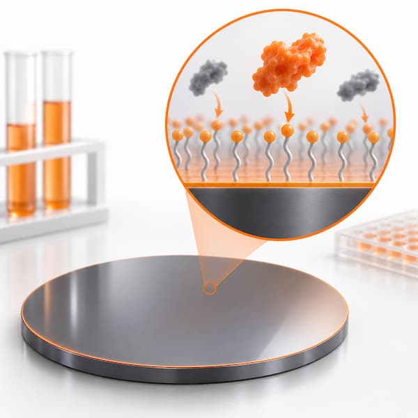
Two common surface routes
Silanization on silicon oxide
Silicon wafers with native or grown oxide can present surface silanol (Si–OH) groups. Organosilanes react at these hydroxylated oxide surfaces to introduce groups such as amines or alkyl chains. For example, APTES is an aminosilane used to introduce amine functionality for further coupling steps. The amount and uniformity of the deposited layer depend on cleaning, available hydroxyl groups, moisture, reagent, and deposition conditions; an APTES treatment should not automatically be assumed to yield a uniform monolayer.1 See our silicon surface chemistry overview and thermal oxide silicon wafers.
Functionalization of oxide-free silicon
Hydrogen-terminated silicon is a different starting surface. Alkene hydrosilylation is one studied route for attaching organic groups through Si–C bonds without an intervening oxide. This chemistry requires a suitable silicon surface preparation and controlled process; it should not be confused with conventional silanization of an oxide layer.2
Choosing a surface for the experiment
- For silicon biosensors and subsequent molecular coupling: specify the intended terminal group, such as amine or carboxyl, and the planned attachment chemistry. Introducing a functional group alone does not verify that a biomolecule has been immobilized.
- For wettability or adhesion studies: specify the treatment and the target measurement. A water contact angle reports wetting behavior but does not by itself establish the chemical identity or uniformity of a layer.
- For electronic interfaces: state whether an oxide is acceptable. An oxide-bearing silane layer and an oxide-free organic layer have different interfacial structures.
Start with the silicon wafer specifications, then identify the oxide condition and final surface chemistry. If a water-repellent coating is the goal, compare the chemistry with our hydrophobic silicon wafer options.
How to verify the modified surface
Choose measurements that answer the specific research question. Spectroscopic ellipsometry can estimate film thickness; X-ray photoelectron spectroscopy (XPS) can probe near-surface elemental composition and chemical states; atomic force microscopy (AFM) can examine topography; and contact-angle measurements assess wettability. A combination of methods is more informative than a single contact-angle reading. Stability in water or under later processing conditions should be checked for the specific coating and protocol.1
Information to include in a quote request
Provide wafer diameter, thickness, crystal orientation, conductivity type and wafer resistivity, polish, oxide type or thickness, desired terminal group, sample quantity, and any acceptance criteria. State whether you need untreated substrates for an in-house process or a specified surface treatment. Surface functionalization is application dependent, so confirm treatment details and testing requirements before ordering.
Request functionalized silicon wafers
Share your wafer and surface specifications in the quote form. Include the surface treatment you plan to perform or request, along with any testing criteria, so the substrate can be matched to your process.
Related silicon wafer resources
- Silicon surface chemistry — hydrophilic and hydrophobic surface behavior.
- Silicon wafer cleaning — preparation considerations before surface treatments.
- Thermal oxide silicon wafers — controlled SiO2 on silicon substrates.
- Hydrophobic silicon wafers — options for water-repellent surfaces.
- Atomic force microscopy on silicon — surface topography and research applications.
Scientific references
- Yadav et al., “Comparative Study of Solution Phase and Vapor Phase Deposition of Aminosilanes on Silicon Dioxide Surfaces”, Materials Science and Engineering C (2014).
- Ciampi et al., “Wet chemical routes to the assembly of organic monolayers on silicon surfaces via the formation of Si–C bonds”, Chemical Society Reviews (2010).