
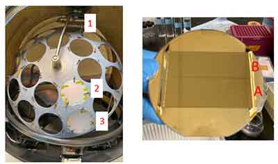
Our lab fabricates SPR chips using gold-coated microscope slides for a custom SPR biosensor. We mount the slides onto used 4 inch silicon wafers before loading them into a CHA Mark 50 e-beam evaporator. We are looking for more low-cost 4 inch wafers for mounting purposes. The wafers do not need to be prime grade because they are not part of the biosensor device.
Silicon Wafers for Biosensor Fabrication
Researchers use silicon wafers for biosensors, SPR chip fabrication, thin-film deposition, porous silicon sensors, photonic biosensors, and e-beam evaporation mounting. For many mounting and carrier wafer applications, low-cost dummy grade or mechanical grade wafers are often a practical choice.
Low-Cost 4 Inch Wafers for SPR Chip Mounting
A researcher needed 4 inch wafers to mount Au-coated microscope slides inside a CHA Mark 50 e-beam evaporator. Since the wafers were used only as mounting supports, prime grade silicon was not required.
UniversityWafer, Inc. Quoted:
Si Item #3342
100mm N/Sb (111) 0.004-0.0025 ohm-cm 381-550um Dummy Grade
Reference #264310 for pricing.
Get Your Silicon Biosensor Wafer Quote FAST! Or, Buy Online and start researching today.
Evaporator-Compatible Materials
For biosensor chip fabrication, researchers may use several wafer and substrate materials inside compatible e-beam evaporation tools. Always confirm the allowed material list for your specific tool before processing wafers, glass slides, metals, organics, or biological samples.
| Allowed Material Categories |
|---|
| Tool Category 1/1E, 2, 3 and 4 materials |
| Silicon-based substrates and films |
| III-V compound semiconductors |
| Glass substrates |
| PECVD and ALD films |
| Cured organics and baked photoresist |
| CNF Class A, B, and refractory metals |
| Exposed gold, silver, and copper |
| Alkali and alkaline compounds |
| Organic/biology molecules prepared with salt buffers |
| High vapor pressure materials such as Mg, Ca, and Zn |
| Soft organic materials |
Related Silicon Biosensor Terms
- Silicon biosensors
- SPR biosensor chips
- Porous silicon sensors
- Nanoporous silicon
- Photonic biosensors
- Silicon interferometers
- Silicon membranes
- Photoluminescent sensors
- Electrochemical etching
- Plasmon spectroscopy
What is a Silicon Biosensor?
A silicon biosensor is a device that uses a silicon-based surface, membrane, porous layer, or photonic structure to detect biological molecules such as proteins, DNA, enzymes, glucose, biomarkers, or cells. Silicon is widely used because it is flat, smooth, chemically functional, compatible with microfabrication, and available in many wafer sizes, dopants, orientations, and surface finishes.
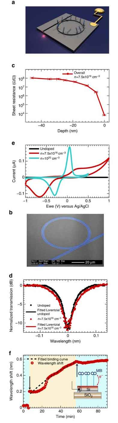 Researchers use silicon wafers as platforms for optical, electrical, electrochemical, and photonic biosensors. The wafer surface can be modified with oxide, nitride, metal films, porous silicon, or biological coatings to create selective binding sites for target molecules.
Why Use Silicon Wafers for Biosensors?
Silicon wafers provide a stable and reproducible base for biosensor fabrication. Their smooth surface allows researchers to deposit thin films, pattern microstructures, create porous layers, and attach biomolecules with controlled surface chemistry.
- Flat, clean surfaces for thin-film deposition and lithography
- Compatible with MEMS, CMOS, photonics, and lab-on-chip processing
- Useful for optical, electrochemical, and label-free biosensing
- Available as prime, test, mechanical, and dummy grade wafers
- Can be coated with gold, oxide, nitride, graphene, or other films
How Do Silicon Biosensors Work?
Silicon biosensors convert a biological interaction into a measurable signal. When a target molecule binds to the functionalized silicon surface, the device may detect a change in refractive index, current, voltage, impedance, photoluminescence, or optical interference.
Common silicon biosensor mechanisms include surface plasmon resonance (SPR), porous silicon photoluminescence, Fabry-Perot interference, field-effect sensing, electrochemical detection, and silicon photonic waveguide sensing.
Examples of Silicon Biosensor Applications
Silicon-based biosensors are used in medical diagnostics, drug discovery, biotechnology, food testing, water quality monitoring, and environmental sensing. They can be designed to detect DNA, proteins, enzymes, bacteria, glucose, oxygen, biomarkers, and other biological targets.
Porous silicon biosensors are especially useful because their high surface area allows biomolecules to attach inside nanoscale pores. Silicon photonic biosensors are also popular for label-free detection because they can detect small refractive-index changes when molecules bind to the sensor surface.
Silicon Wafers for SPR and E-Beam Evaporation
Silicon wafers are also used as carrier wafers or mounting substrates during biosensor chip fabrication. For example, researchers may mount glass slides or SPR chips onto 4 inch silicon wafers before loading them into an e-beam evaporator for gold or metal film deposition.
For this type of work, expensive prime grade wafers are not always required. Many labs use lower-cost dummy grade silicon wafers, test wafers, or mechanical grade wafers when the wafer is only used for mounting, handling, or process support.
Porous Silicon Biosensors
Porous silicon is commonly used in biosensor research because its nanoscale pore structure increases surface area and improves molecule immobilization. Depending on the substrate type and etching conditions, porous silicon can be engineered for optical, electrochemical, or photoluminescent biosensing.
Porous silicon biosensors may be used to detect DNA hybridization, enzyme reactions, bacteria, metabolites, or other biological molecules. Changes in the porous layer can shift optical signals, alter electrical response, or change photoluminescence intensity.
What is a Fabry-Perot Fringe Pattern?
A Fabry-Perot fringe pattern is an optical interference pattern that can be used to detect changes on or inside a silicon biosensor. In porous silicon biosensors, binding events can change the refractive index of the porous layer, causing a measurable shift in the interference pattern.
This makes Fabry-Perot-based silicon biosensors useful for label-free detection of biomarkers, DNA, proteins, and other biological analytes.
Order Silicon Wafers for Biosensor Research
UniversityWafer, Inc. supplies silicon wafers for biosensor fabrication, SPR chip mounting, porous silicon research, photonic biosensors, MEMS devices, and e-beam evaporation processes. Researchers can request prime, test, dummy, oxide-coated, nitride-coated, or custom silicon wafers for their project requirements.