
Request a Quote for GaN on Sapphire Wafers
UniversityWafer supplies GaN on sapphire wafers for university, government, and industrial research involving HEMTs, RF electronics, power semiconductor devices, LEDs, laser diodes, and UV photodetectors. We offer both standard inventory and custom gallium nitride epitaxial wafers with various substrate materials, epitaxial layer thicknesses, wafer diameters, and doping options. Complete the form below to receive a fast quotation from our technical team.
Standard GaN on Sapphire Wafer

Gallium Nitride (GaN) on sapphire is one of the most common epitaxial structures used for research involving high-power electronics, LEDs, laser diodes, ultraviolet photodetectors, RF components, and wide bandgap semiconductor devices. UniversityWafer supplies both standard inventory and custom-grown GaN epitaxial wafers.
Typical Specifications
| Property | Typical Value |
|---|---|
| Substrate | Sapphire (Al₂O₃) |
| Wafer Diameter | 50 mm (custom sizes available) |
| Conductivity Type | N-Type |
| GaN Thickness | 0.5–10 μm |
| Orientation | On-Axis |
| Applications | HEMTs, LEDs, UV devices, RF electronics, power semiconductors |
Custom Epitaxial Wafer Solutions
Need different GaN thicknesses, substrate materials, doping levels, wafer diameters, or multilayer structures such as GaN/AlN/Sapphire or GaN/AlN/SiC? Contact UniversityWafer for custom epitaxial wafer solutions designed for your research project.
GaN on Sapphire Wafers for Semiconductor and Optoelectronic Research
Gallium Nitride (GaN) on sapphire wafers are among the most widely used wide bandgap semiconductor substrates for research involving high-power electronics, high-frequency RF devices, ultraviolet LEDs, laser diodes, photodetectors, and next-generation power semiconductors. UniversityWafer supplies high-quality GaN epitaxial wafers grown on sapphire, aluminum nitride (AlN), and silicon carbide (SiC) substrates for universities, government laboratories, and commercial R&D facilities.
The combination of GaN's high breakdown voltage, excellent thermal stability, high electron mobility, and wide bandgap enables devices capable of operating at higher voltages, higher temperatures, and faster switching speeds than conventional silicon technologies.
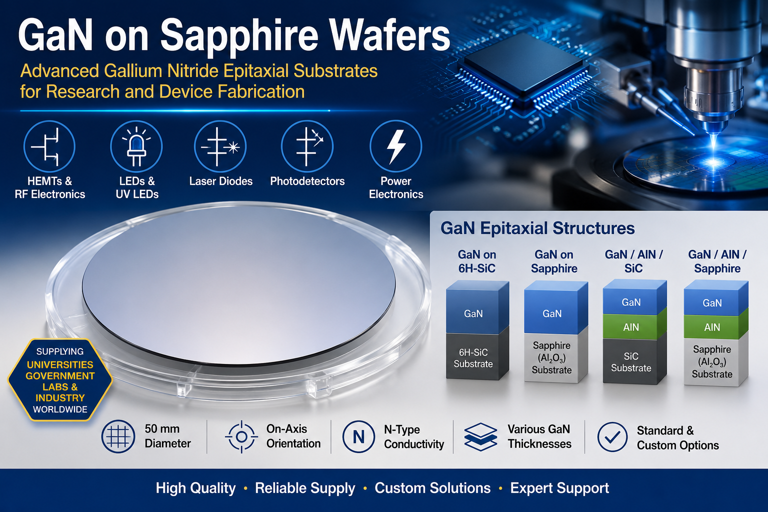
Available GaN Epitaxial Wafer Configurations
| Structure | Typical Epitaxial Structure | Common Research Applications |
|---|---|---|
| GaN on 6H-SiC |
50 mm diameter On-axis N-type GaN thickness: approximately 0.5 µm |
HEMTs, RF power amplifiers, microwave devices, and high-power electronics |
| GaN on Sapphire |
50 mm diameter On-axis N-type GaN thickness: 0.5–10 µm |
LEDs, UV LEDs, laser diodes, photodetectors, and optoelectronic research |
| GaN / AlN / SiC |
50 mm diameter On-axis N-type GaN thickness: 0.5–0.8 µm AlN thickness: approximately 0.1 µm |
High-frequency electronics, HEMTs, RF devices, and microwave research |
| GaN / AlN / Sapphire |
50 mm diameter On-axis N-type GaN thickness: 0.5–0.8 µm AlN thickness: approximately 0.1 µm |
III-nitride research, power electronics, LEDs, and UV optoelectronics |
Why Researchers Choose GaN on Sapphire
Sapphire remains one of the most popular substrates for GaN epitaxial growth because it offers excellent chemical stability, high-temperature compatibility, and a cost-effective platform for producing high-quality nitride semiconductor layers. Although silicon carbide provides superior thermal conductivity, sapphire continues to be the preferred substrate for many LED, photonics, and academic research applications.
Whether your research involves HEMT fabrication, high-frequency RF electronics, UV photodetectors, power switching devices, laser diodes, or advanced III-nitride semiconductor structures, UniversityWafer can provide standard or custom GaN on sapphire wafers to meet your project requirements.