
What Is Germanium-on-Insulator (GOI)?
Germanium-on-Insulator (GOI) is an engineered semiconductor substrate consisting of a thin crystalline germanium (Ge) device layer separated from a supporting substrate by an electrically insulating layer. The architecture is conceptually similar to Silicon-on-Insulator (SOI), but replaces the silicon device layer with germanium to take advantage of germanium's electronic and optical properties.
Germanium has significantly higher intrinsic electron and hole mobility than silicon, making GOI attractive for researchers developing high-speed transistors, advanced CMOS architectures, photonic devices, and low-power electronics.
The buried insulating layer also provides electrical isolation between the active germanium layer and the underlying substrate, which can help reduce parasitic capacitance and support specialized device structures.
Why Use Germanium on an Insulator?
Combining germanium with an insulating layer provides researchers with several potential advantages:
- High carrier mobility for high-speed electronic device research
- Strong infrared absorption useful for optical detection
- Electrical isolation of the active device layer
- Reduced parasitic capacitance in appropriate device architectures
- Compatibility with research into CMOS and silicon-based integration
- Thin germanium device layers suitable for nanofabrication
- Opportunities for integrating electronic and photonic components on a common platform
These characteristics make GOI particularly interesting where conventional bulk silicon or bulk germanium substrates cannot provide the desired combination of electrical isolation and material performance.
GOI for Silicon Photonics
One of the most important research areas for GOI is silicon photonics. Germanium is useful for near-infrared optoelectronics because its optical properties allow it to interact with wavelengths important to optical communication systems.
Thin germanium layers can be incorporated into photonic device architectures for research involving:
- Near-infrared photodetectors
- Integrated optical receivers
- Optical communication devices
- Waveguide-integrated detectors
- Photonic integrated circuits (PICs)
- On-chip optical interconnects
GOI therefore provides a useful experimental platform for researchers investigating the integration of germanium photonics with silicon semiconductor technology.
High-Mobility Electronic Devices
Germanium is also investigated as an alternative channel material for advanced transistor architectures. Its high carrier mobility can potentially enable devices with strong electrical performance at reduced operating voltages.
GOI substrates may be used to investigate:
- MOSFET and CMOS devices
- Germanium-channel transistors
- FinFET and advanced transistor structures
- Low-power electronics
- High-frequency devices
- Thin-body semiconductor devices
- Next-generation logic architectures
The insulating layer can be especially useful for thin-body devices where researchers need greater control over the active semiconductor region.
Infrared Detectors and Sensors
Germanium's optical response makes GOI attractive for infrared detector and sensor research. Germanium has a bandgap of approximately 0.66 eV at room temperature and can absorb portions of the near-infrared spectrum that crystalline silicon does not efficiently detect.
Potential GOI research applications include near-infrared photodetectors, optical sensors, spectroscopy components, imaging technologies, and integrated optoelectronic devices.
GOI Wafer Research Applications
Germanium-on-Insulator substrates can support research across semiconductor physics, photonics, electronics, and nanotechnology. Applications may include:
- Silicon and germanium photonics
- Near-infrared photodetectors
- High-speed transistors
- CMOS integration research
- Optoelectronic devices
- Thin-film semiconductor research
- MEMS and sensor development
- Nanostructures and nanofabrication
- Material characterization
- Semiconductor process development
Researchers can use GOI substrates to study how germanium behaves when confined to thin active layers and integrated with insulating and semiconductor materials.
Get Your Germanium-on-Insulator (GOI) Quote FAST! Or, Buy Wafers Online and Start Researching Today!
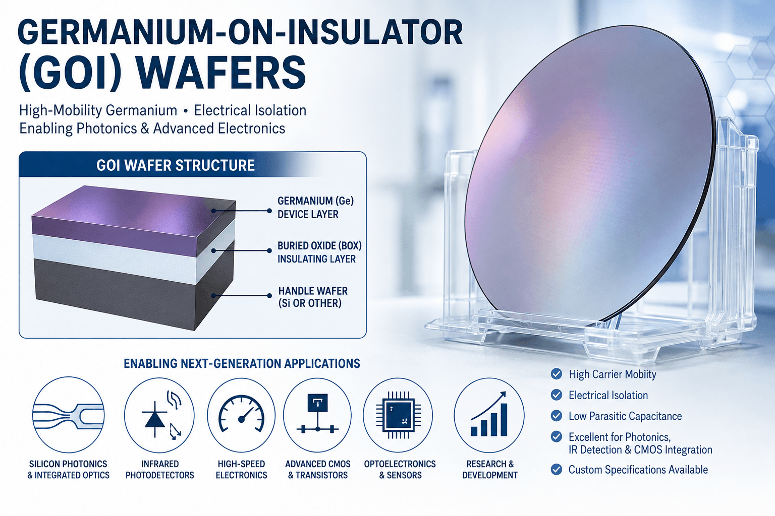
Germanium-on-Insulator Wafer Structure
A typical Germanium-on-Insulator (GOI) wafer uses a layered structure designed to isolate a thin crystalline germanium device layer from the supporting substrate. Depending on the fabrication method and research requirements, the structure may include:
- Germanium device layer – the active semiconductor layer used for device fabrication
- Buried oxide (BOX) – an electrically insulating dielectric layer, commonly based on SiO2
- Handle wafer – provides mechanical support for the thin device and insulating layers
The thickness of each layer can be selected according to the intended research application. Thin germanium device layers are particularly useful for advanced electronic and photonic device structures.
GOI vs. Bulk Germanium Wafers
Both GOI and germanium wafers provide access to the useful electrical and optical properties of crystalline Ge, but their structures are significantly different.
Bulk germanium wafers consist primarily of germanium throughout the substrate, while GOI places a comparatively thin Ge device layer above an insulating layer. This configuration allows researchers to combine germanium's material properties with the electrical isolation provided by the buried dielectric.
Bulk Ge may be preferred for applications requiring a thick germanium substrate, while GOI can be advantageous for thin-film devices, integrated photonics, advanced transistor architectures, and research requiring electrical isolation.
GOI vs. Germanium-on-Silicon (GeOSi)
Germanium-on-Insulator should also be distinguished from Germanium-on-Silicon (GeOSi) wafers.
In a GeOSi substrate, crystalline germanium is typically grown or deposited on a silicon substrate. In GOI, the germanium device layer is separated from the handle substrate by an insulating layer.
- GOI: Ge device layer / insulating layer / handle substrate
- GeOSi: Ge layer / silicon substrate
- SOI: Si device layer / buried oxide / silicon handle substrate
The appropriate structure depends on the electrical, optical, thermal, and fabrication requirements of the device being developed.
Germanium and SOI Technology
GOI shares important structural concepts with Silicon-on-Insulator (SOI) wafers for photonics. Both platforms use an insulating layer beneath a thin semiconductor device layer to create specialized electronic or optical structures.
Germanium can provide capabilities that complement silicon, particularly for infrared detection and high-mobility electronic research. This makes GOI interesting for researchers investigating heterogeneous integration of germanium with established silicon semiconductor and photonic technologies.
GOI for Photodetector Fabrication
One promising application of Germanium-on-Insulator is the fabrication of near-infrared photodetectors. Germanium can absorb near-infrared wavelengths used in many optical communication systems, allowing Ge-based detector structures to be incorporated into integrated photonic platforms.
Potential devices include:
- Waveguide-integrated photodetectors
- Near-infrared optical detectors
- Integrated optical receivers
- Photonic integrated circuits
- Optical communication components
- On-chip optical sensors
GOI for Advanced Transistor Research
The high carrier mobility of germanium has also made it an important material for research into next-generation transistor technologies. Thin-body GOI structures may be investigated for devices where researchers require both a high-mobility semiconductor channel and electrical isolation from the underlying substrate.
Research areas can include Ge MOSFETs, CMOS integration, FinFETs, thin-body transistors, high-frequency electronics, and low-power semiconductor devices.
GOI Wafer Specifications to Consider
When requesting Germanium-on-Insulator wafers, researchers should provide as much information as possible about the required substrate. Important specifications can include:
- Wafer diameter
- Germanium device-layer thickness
- Buried oxide (BOX) thickness
- Germanium crystal orientation
- Dopant type
- Resistivity
- Handle wafer material and thickness
- Surface finish
- Surface roughness requirements
- Quantity required
Providing detailed specifications helps determine the most appropriate GOI structure for your semiconductor, photonic, infrared, or materials research.
Germanium-on-Insulator for Research & Development
GOI is an important experimental substrate for researchers exploring the intersection of germanium electronics, silicon photonics, infrared detection, and advanced semiconductor integration.
UniversityWafer supplies semiconductor substrates for universities, laboratories, device developers, and semiconductor researchers. Contact us with your required GOI device-layer thickness, BOX thickness, wafer diameter, orientation, surface condition, and quantity for availability and pricing.
Related Germanium & Semiconductor Resources
- Germanium (Ge) Wafers – Explore germanium substrates for infrared optics, photonics, detectors, and advanced semiconductor research.
- Germanium-on-Silicon (GeOSi) Wafers – Learn about epitaxial germanium layers on silicon for photonics, transistors, infrared devices, and optoelectronics.
- Germanium-on-Insulator (GeOI) Substrates – View additional GOI wafer specifications and examples for semiconductor research.
- SOI Wafers for Photonic Devices – Learn how Silicon-on-Insulator substrates are used for waveguides, photonic integrated circuits, modulators, and optical devices.
- Integrated Photonics Substrates – Compare substrate materials used for photonic integrated circuits, optical communication, sensors, and quantum photonics.
- Electrical Grade Germanium Wafers – Germanium substrates for high-speed electronics, photodetectors, semiconductor devices, and photonics.