Custom Germanium Wafers for Research and Device Development
UniversityWafer supplies germanium wafers (Ge wafers) for universities,
research laboratories, aerospace and defense research, photonics, detector development,
and semiconductor applications. Germanium substrates can be selected according to
crystal orientation, conductivity type, resistivity, thickness, diameter, surface finish,
and intended use.
Because optical, electronic, photovoltaic, and detector applications can require very
different material properties, the most suitable germanium wafer depends on the specific
device or experiment. Providing detailed specifications with your request helps identify
the best substrate for your application.
Typical Germanium Wafer Specifications
- Material grade: optical-grade or electrical-grade germanium
- Crystal orientation: commonly <100>, <111>, or specialized orientations
- Conductivity type: P-type, N-type, or high-resistivity / nominally intrinsic material
- Electrical specification: resistivity or dopant concentration as required
- Surface finish: single-side polished (SSP) or double-side polished (DSP)
- Dimensions: custom diameter and thickness requirements
- Surface quality: polishing, roughness, and finish requirements depending on application
- Quantity: research quantities through larger-volume orders
What Information Should You Include in a Germanium Wafer Request?
For the fastest and most accurate quote, include as many of the following specifications
as possible:
- Wafer diameter
- Wafer thickness
- Crystal orientation
- P-type, N-type, or high-resistivity material
- Required resistivity or dopant concentration
- Single-side or double-side polish
- Surface roughness or optical finish requirements
- Quantity required
- Intended application or process
Germanium Wafers for Optical Applications
For infrared optical work, important specifications may include surface polish, optical
quality, wafer thickness, diameter, flatness, and the wavelength range of interest.
Optical performance can vary with material quality, wavelength, temperature, surface
condition, and any coating applied to the finished optic.
Germanium Wafers for Semiconductor Research
Electronic and semiconductor applications may require tighter control of
crystal orientation, resistivity, conductivity type, surface preparation, and
dimensional tolerances. These parameters can influence epitaxy, interface
formation, device fabrication, and electrical characterization.
Germanium Wafers for Epitaxy
Germanium substrates are used in selected epitaxial research, including work involving
III-V materials and heterostructures. For epitaxial applications, crystal orientation,
surface preparation, miscut requirements, polishing quality, and substrate cleanliness
may be important to the growth process.
Germanium for Detector and Photonics Research
Germanium is used in photodetector, infrared, and photonics research because of its
electronic and optical properties. However, detector requirements vary significantly
between applications. For example, high-purity germanium used in radiation spectroscopy
has much more specialized purity requirements than a standard semiconductor research
wafer.
Common Germanium Wafer Applications
- Infrared optics and thermal imaging research
- Near-infrared photodetectors
- Silicon photonics and Ge-on-Si research
- III-V epitaxial growth and heterostructure research
- Multi-junction photovoltaic devices
- High-mobility semiconductor device research
- Radiation detector material research
- Surface science and semiconductor characterization
Request a Germanium Wafer Quote
Complete the form below with your required diameter, thickness, orientation,
conductivity type, resistivity, polish, quantity, and application. If you are
unsure which specification is appropriate, include information about your process or
research objective so the available germanium substrate options can be evaluated.
Get Your Germanium Wafer Quote FAST!
Or,
Buy Online
and Start Researching Today!
Why Choose Germanium Wafers?
Germanium (Ge) is a group IV semiconductor used in infrared optics,
photonics, detectors, high-speed electronic research, and advanced photovoltaic devices.
At room temperature, crystalline germanium has an indirect bandgap of approximately
0.66 eV, which is smaller than that of silicon. Germanium also has higher
electron and hole mobilities than silicon, making it attractive for research involving
high-speed and low-voltage semiconductor devices.
Optical-grade germanium is particularly important for mid-infrared optical
applications because properly prepared germanium can provide useful transmission
over a broad infrared wavelength range while also having a high refractive index.
Electrical-grade material, meanwhile, can be selected by conductivity type, resistivity,
crystal orientation, thickness, and surface finish for semiconductor and device research.
UniversityWafer supplies germanium wafers and Ge substrates for research,
prototype development, optics, detectors, photovoltaics, and semiconductor processing.
Available specifications may include custom diameters, orientations, doping types,
resistivities, thicknesses, and single- or double-side polished surfaces.
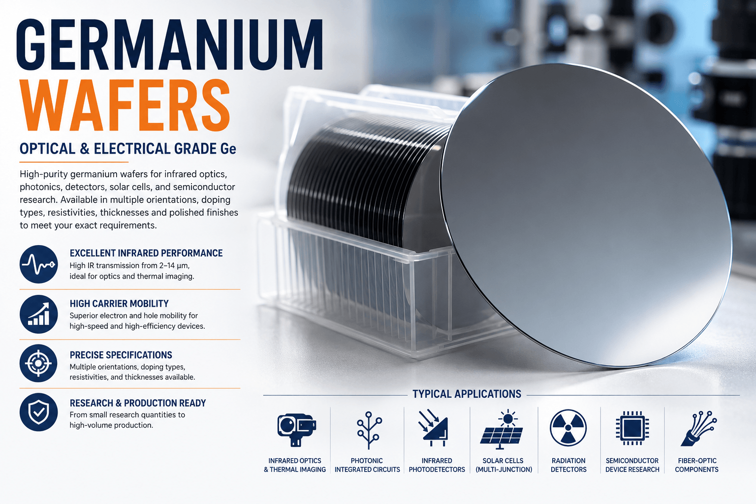
Common Applications of Germanium Wafers
- Infrared optics: windows, lenses, filters, and other components for selected mid-infrared systems
- Thermal imaging: optical components used in infrared imaging and sensing systems
- Photodetectors: germanium-based detection research, particularly at near-infrared telecommunications wavelengths
- Silicon photonics: research involving germanium or Ge-on-Si structures for optical detection and integration
- Multi-junction solar cells: germanium substrates used in high-efficiency III-V photovoltaic structures
- Radiation detection: high-purity germanium materials used in gamma-ray and X-ray detector technologies
- High-speed electronics: research into transistors and devices that benefit from germanium's high carrier mobility
- Semiconductor research: epitaxy, heterostructures, surface studies, and device development
Germanium Wafer Properties
The properties that make germanium useful depend on the application. Optical systems
typically emphasize infrared transmission, surface quality, thickness, and optical
uniformity, while electronic applications may require tight control of resistivity,
dopant type, orientation, and crystal quality.
| Property |
Germanium |
Silicon |
| Indirect Bandgap at Room Temperature |
Approximately 0.66 eV |
Approximately 1.12 eV |
| Electron Mobility |
Higher than silicon |
Lower than germanium |
| Hole Mobility |
Higher than silicon |
Lower than germanium |
| Infrared Optical Use |
Widely used for selected near- and mid-infrared applications |
Useful in selected infrared wavelength ranges |
| Refractive Index |
High in the infrared |
Also high, but generally lower than germanium in comparable IR regions |
| Thermal Conductivity |
Lower than silicon |
Higher than germanium |
| Typical Research Uses |
IR optics, photodetectors, III-V solar cells, high-mobility devices |
Integrated circuits, MEMS, sensors, power devices, photonics |
Optical-Grade vs. Electrical-Grade Germanium
Optical-Grade Germanium
Optical-grade germanium is selected for infrared applications where surface quality,
optical transmission, thickness, and polishing are important. Depending on the optical
system, substrates may be fabricated into windows, lenses, filters, or other infrared
components. Anti-reflection coatings are often used in finished germanium optics because
germanium has a high refractive index and therefore significant Fresnel reflection from
an uncoated surface.
Electrical-Grade Germanium
Electrical-grade germanium is used in semiconductor and electronic research where
properties such as conductivity type, dopant concentration, resistivity, crystal
orientation, and surface preparation can influence device performance and
processing results.
Germanium Wafer Crystal Orientations
Germanium wafers may be supplied in common crystallographic orientations such as
<100> and <111>, with other orientations available
for specialized research. Crystal orientation can affect epitaxial growth, surface
chemistry, etching behavior, interface formation, and device fabrication.
P-Type, N-Type, and Intrinsic Germanium
Germanium substrates can be supplied as P-type, N-type, or high-resistivity /
nominally intrinsic material, depending on the intended application. Dopant type
and concentration determine electrical conductivity and should be selected according to
the device structure, epitaxial process, detector design, or electrical measurements
being performed.
Germanium for Infrared Optics
Germanium is widely used in infrared optical systems because of its favorable transmission
in selected infrared wavelength regions and its high refractive index. Applications can
include thermal imaging, infrared spectroscopy, sensing systems, and other IR optical
assemblies.
Optical performance depends on the material grade, impurity content, surface finish,
thickness, wavelength, operating temperature, and any applied optical coating. For this
reason, the correct germanium specification should be selected for the intended optical
band rather than assuming that all Ge substrates provide identical transmission.
Germanium for Photodetectors and Photonics
Germanium is important in photonics because it can absorb near-infrared wavelengths used
in telecommunications and can be integrated with silicon-based platforms. Germanium and
Ge-on-Si structures are therefore widely studied for photodetectors, optical receivers,
and silicon photonic devices.
Bulk germanium wafers can also serve as research substrates for epitaxy, material
characterization, detector development, and related photonic experiments.
Germanium Substrates for Multi-Junction Solar Cells
Germanium is commonly used as a substrate in high-efficiency III-V multi-junction
solar cells. Its lattice constant is closely matched to materials such as GaAs,
which makes it useful as a foundation for epitaxial III-V device structures. In some
multi-junction designs, the germanium substrate can also contribute as the lowest-bandgap
junction.
Available Germanium Wafer Specifications
Germanium substrates can be supplied in a range of configurations depending on the
application. Important specifications may include:
- Optical-grade or electrical-grade germanium
- <100>, <111>, and specialized crystal orientations
- P-type, N-type, or high-resistivity / nominally intrinsic material
- Specified resistivity or dopant concentration
- Single-side polished (SSP) or double-side polished (DSP) surfaces
- Custom wafer diameters and thicknesses
- Thickness tolerance and total thickness variation requirements
- Surface roughness and polishing requirements
- Research quantities through larger production orders
How to Select a Germanium Wafer
When requesting a germanium substrate, consider the requirements of the experiment or
device before selecting the wafer specification.
- Application: optical, electronic, photovoltaic, detector, or epitaxial research
- Diameter: select a size compatible with your equipment and process
- Thickness: consider mechanical strength, optical path length, and processing requirements
- Orientation: choose the crystal plane required for epitaxy, etching, or device fabrication
- Conductivity type: P-type, N-type, or high-resistivity material as required
- Resistivity: specify the electrical range needed for the experiment
- Surface finish: SSP or DSP depending on optical, bonding, epitaxial, or device requirements
- Optical requirements: specify the wavelength range and surface quality for infrared applications
Custom Germanium Substrates
If your project requires a non-standard germanium wafer, UniversityWafer can help source
substrates with application-specific specifications. Custom requirements may include
diameter, orientation, thickness, resistivity, doping, polish, surface quality, and other
dimensional or material parameters.
When requesting a quote, provide as much information as possible about the intended
application and required specifications so the appropriate germanium substrate can be
identified.
Related Germanium and Semiconductor Resources
-
Silicon Wafers
– Compare germanium with the most widely used semiconductor substrate.
-
III-V Semiconductor Wafers
– Explore compound semiconductor materials used in photonics, electronics, and multi-junction solar cells.
-
Photonic Device Substrates
– Learn about substrates used for photodetectors, optical devices, and integrated photonics research.
-
Photodiode Research
– Explore semiconductor materials used in photodetection and optical sensing applications.
-
Solar Cell Wafers
– Learn about semiconductor substrates used in photovoltaic and multi-junction solar cell research.
-
Wafer Processing Services
– Explore wafer polishing, processing, and customization options.
-
What Is a Semiconductor Wafer?
– Learn how semiconductor wafers are manufactured and used in research and device fabrication.
