Photodiodes and Their Fabrication Substrates
Photodiodes are semiconductor devices that convert light into electrical signals and are essential components in fiber-optic communications, medical imaging, industrial sensors, LiDAR, spectroscopy, solar energy, and scientific instrumentation. This guide explains how photodiodes work, compares the most common photodiode types, and explores the semiconductor wafers and materials used to fabricate high-performance photodetectors, including silicon, germanium, GaAs, InGaAs, InP, SiC, and GaN.
Need Silicon Wafers for Photodiode Fabrication?
UniversityWafer supplies silicon wafers, SOI wafers, epitaxial silicon wafers, and custom semiconductor substrates for researchers developing photodiodes, photodetectors, solar cells, image sensors, and other optoelectronic devices. Whether you need prime-grade silicon, buried oxide structures, custom doping, or complete epitaxial stacks, our engineering team can help identify the best substrate for your application.
The following inquiry came from a university postdoctoral researcher developing photodiodes using SOI technology.
"I was wondering if you sold wafers used for solar cell or photodiode processing. We are looking for pre-doped wafers that only require metallization and dicing."
"We need a 3-inch SOI wafer with a boron-doped epitaxial silicon layer, <100> orientation, resistivity of 1–5 Ω·cm, an epi thickness below 1 µm, and a buried oxide between 0.5 and 1 µm."
"Can the buried oxide be produced using the SIMOX ion implantation process?"
UniversityWafer Response
Yes. UniversityWafer regularly supplies SOI substrates, epitaxial silicon wafers, and custom silicon substrates for photodiode fabrication. SIMOX-produced buried oxide layers, custom resistivity, crystal orientation, wafer diameter, polishing, and epitaxial specifications can all be supplied depending on your research requirements.
Reference #140678 contains the quoted specifications and pricing for this project.
Get Your Photodiode Wafer Quote FAST!
Or,
Buy Online
and start fabricating today!
What Is A Photodiode?
A photodiode is a semiconductor device that converts light into an electrical current. It operates by allowing photons (light particles) to hit the photodiode's semiconductor material (often silicon or germanium), generating electron-hole pairs. This process creates a current directly proportional to the intensity of the incoming light.

Photodiodes are widely used in applications requiring precise light detection, such as: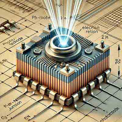
- Optical communication systems: Converting light signals into electrical signals.
- Photometry and radiometry: Measuring light intensity in scientific instruments.
- Solar cells: A specific type of large photodiode used to generate power.
- Safety and sensing: Detecting motion or presence through light interruption or reflection.
There are different types of photodiodes, such as PIN diodes and avalanche photodiodes, each suited to specific applications based on their sensitivity, response time, and noise characteristics.
Bonding Silicon Carbide to Fabricate Photodiodes
A corporate researcher requested a quote for the following.
We are looking to wafer bond these together build a photodiode. I seen on the attached excel file university wafer has available:
4H-N 3" dia,
Type/ Dopant : N / Nitrogen
Orientation :4 degree+/-0.5 degree
Thickness : 350 ± 25 um
B Grade,MPD<30 cm-2
B Grade,RT:0.01-0.1Ω·cm
B Grade,Bow/Warp/TTV<35um
Double face polished/Si face epi-ready with CMP,Surface Roughness : <0.5 nm
Reference #167250 for specs and pricing.
Types of Photodiodes
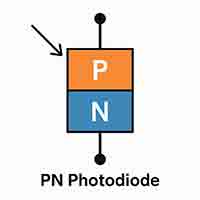
PN Photodiode
A PN photodiode converts photons into electrical current using a p-n junction, ideal for low-speed, low-cost light detection applications.
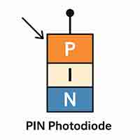
PIN Photodiode
A PIN photodiode features an intrinsic layer for higher sensitivity, faster response, and broader bandwidth, perfect for optical communication.
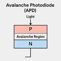
Avalanche Photodiode
APDs amplify light signals internally, offering ultra-high sensitivity for LIDAR systems, low-light detection, and medical imaging.
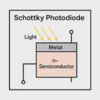
Schottky Photodiode
Schottky photodiodes use a metal-semiconductor junction for fast, low-capacitance detection, great for high-frequency and UV applications.
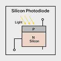
Silicon Photodiode
Silicon photodiodes detect visible and near-infrared light, widely used in optical sensors, barcode scanners, and solar devices.
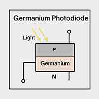
Germanium Photodiode
Germanium photodiodes specialize in infrared detection (800–1800nm), essential for fiber optic communication and thermal imaging.
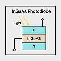
InGaAs Photodiode
InGaAs photodiodes deliver high quantum efficiency for near-IR and SWIR detection, key in spectroscopy and fiber optic testing.
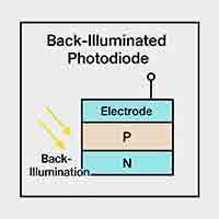
Back-Illuminated Photodiode
Back-illuminated photodiodes maximize light absorption by placing electrodes behind the active area, enhancing imaging sensitivity.
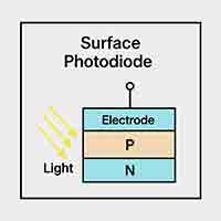
Surface Photodiode
Surface photodiodes are designed for short-wavelength light detection, ideal for optical encoders and laser monitoring systems.
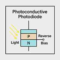
Photoconductive Photodiode
Photoconductive photodiodes operate in reverse bias to enhance speed and sensitivity, perfect for optical receivers and LIDAR.
Substrates for Photodiode Fabrication
The performance of a photodiode is largely determined by the semiconductor substrate used during fabrication. Material selection influences wavelength sensitivity, response speed, quantum efficiency, dark current, and operating temperature. Depending on the application, photodiodes may be fabricated on silicon, germanium, gallium arsenide (GaAs), InGaAs, InP, SiC, GaN, and other advanced semiconductor materials. Choosing the proper substrate ensures the finished photodiode is optimized for its target wavelength range and operating environment.
-
Silicon (Si)
- The industry standard for photodiodes operating in the visible and near-infrared spectrum (approximately 400–1,100 nm).
- Manufactured using high-quality silicon wafers with mature fabrication processes that provide excellent yield and low production costs.
- Commonly used in cameras, optical sensors, barcode scanners, medical devices, industrial automation, and photodetector systems.
-
Germanium (Ge)
- Offers extended sensitivity into the near-infrared region up to approximately 1,800 nm.
- Frequently selected for fiber-optic receivers, infrared instrumentation, and scientific imaging systems.
- Although more expensive than silicon, germanium remains valuable where longer wavelength detection is required.
-
Gallium Arsenide (GaAs)
- Provides high electron mobility and excellent high-frequency performance.
- Often used in high-speed optical communications, aerospace electronics, and defense applications.
- GaAs substrates are also widely used for fabricating advanced optoelectronic devices and high-speed semiconductor components.
-
Indium Gallium Arsenide (InGaAs)
- Ideal for short-wave infrared (SWIR) detection from approximately 900 to 2,600 nm.
- Typically grown on InP substrates using MOCVD or other epitaxial growth techniques.
- Widely used in fiber-optic communications, LiDAR, spectroscopy, biomedical imaging, machine vision, and infrared cameras.
-
Indium Phosphide (InP)
- Provides exceptional electron mobility and thermal stability for high-speed photodiodes.
- Commonly serves as the substrate for InGaAs detector structures operating at telecommunications wavelengths of 1,310 and 1,550 nm.
- Frequently selected for optical networking, data centers, and advanced photonic integrated circuits.
-
Cadmium Telluride (CdTe) and Cadmium Zinc Telluride (CdZnTe)
- Engineered for detecting high-energy X-ray and gamma-ray photons.
- Their high atomic numbers improve photon absorption efficiency compared with silicon-based detectors.
- Used in medical imaging, homeland security, industrial inspection, and astrophysics instrumentation.
-
Silicon Carbide (SiC) and Gallium Nitride (GaN)
- Wide-bandgap semiconductors designed for ultraviolet (UV) photodetection.
- Offer outstanding radiation hardness, chemical stability, and high-temperature operation.
- Ideal for flame detection, UV astronomy, environmental monitoring, aerospace electronics, and harsh-environment sensing.
Whether your project requires a standard silicon wafer, an epitaxial substrate, or advanced III-V semiconductor materials such as GaAs, InGaAs, or InP, selecting the correct substrate is the first step toward achieving high sensitivity, fast response time, and reliable photodiode performance.
Related Photodiode & Semiconductor Resources
