
Sapphire vs Silicon Wafers. Which Is Best For Manufacturing Optoelectronic Devices?
Optoelectronic devices rely heavily on the choice of wafer material for their performance, with silicon and sapphire representing two dominant yet contrasting options in this cutting-edge field. The unique crystal structures and atomic arrangements of these materials directly influence how they interact with light, electricity, and heat—critical factors that determine their suitability across various applications. Engineers and researchers developing next-generation technologies must carefully weigh the trade-offs between silicon's semiconductor properties and cost-effectiveness against sapphire's exceptional optical transparency and mechanical durability. While silicon has long been the backbone of conventional electronics, sapphire is increasingly vital for specialized applications requiring superior light transmission and resilience in harsh environments. The expanding optoelectronics market, projected to reach $88.5 billion by 2028, continues to drive innovation in both materials, pushing manufacturers to refine production techniques and enhance performance characteristics. Understanding the distinctive advantages and limitations of each wafer type enables designers to make informed decisions that can significantly impact device efficiency, reliability, and commercial viability in this rapidly evolving technological landscape.
Get Your Quote FAST! Or, Buy Online and Start Researching Today!
Sapphire vs. Silicon Wafers: Key Takeaways
| Property | Silicon Wafers | Sapphire Wafers |
|---|---|---|
| Electrical Conductivity | Semiconductor (controllable) | Insulator |
| Optical Transparency | Opaque to visible, transparent to IR | Transparent to UV-IR |
| Thermal Conductivity | High | Moderate |
| Hardness | Moderate | Very high (9 on Mohs scale) |
| Cost | Lower | Higher |
| Primary Applications | Electronics, IR sensors | LEDs, optical windows |
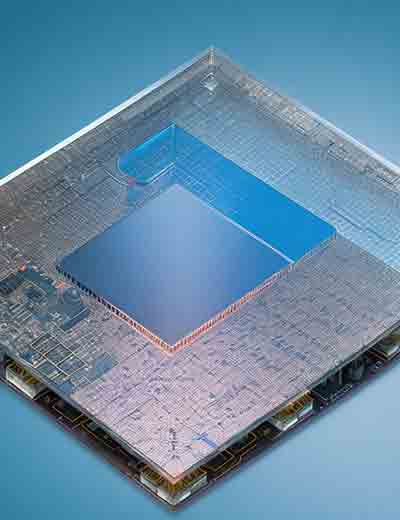
Understanding Silicon Wafers
Silicon wafers are the foundation of the semiconductor industry. They're made from very pure silicon that's melted and formed into large crystals, then sliced into thin, round wafers. This process has been improved for decades, resulting in high-quality substrates for electronic devices.
Silicon wafers have some great qualities for electronics:
- They're excellent semiconductors, which means we can control how well they conduct electricity. This is key for making transistors and integrated circuits.
- They're really good at handling heat, which is important for high-performance electronic devices that get hot when they work.
- We can easily change their properties by adding tiny amounts of other materials (called doping).
- They're much cheaper to make than other types of wafers.
- Silicon wafers can be made in large sizes, which helps make chip production more efficient and cheaper.
Choosing the right silicon wafer is crucial for getting the best performance in your devices. Things like crystal orientation, dopant type and concentration, and surface finish all matter for specific applications.
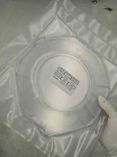
Exploring Sapphire Wafers
Sapphire wafers are made from synthetic sapphire, which is a crystal form of aluminum oxide. They're not the same as the sapphires in jewelry, but they do share some similar properties. Making sapphire wafers involves special crystal growth techniques.

Sapphire wafers have some unique features:
- They're incredibly hard (almost as hard as diamond), which makes them very scratch-resistant.
- They can handle very high temperatures without losing their shape or properties.
- They're see-through to a wide range of light, including ultraviolet, visible, and infrared.
- They're great insulators, which means they don't conduct electricity easily.
- Sapphire doesn't corrode easily, even when exposed to many harsh chemicals.
These properties make sapphire wafers perfect for certain types of optoelectronic devices, especially those that need to work with light across a broad spectrum or operate in tough environments.
Comparing Silicon and Sapphire Wafers
| Property | Silicon Wafers | Sapphire Wafers |
|---|---|---|
| Electrical Properties | Semiconductor - controllable conductivity, ideal for transistors and electronic components | Insulator - poor electrical conductor, useful for preventing signal interference |
| Optical Properties | Opaque to visible light, works with infrared light | Transparent across wide range (UV to infrared), ideal for optical applications and LEDs (especially blue and UV) |
| Thermal Characteristics | Better heat conductor, helps with device cooling | Higher temperature tolerance without degradation, suitable for extreme temperature environments |
| Mechanical Strength | Strong but less hard, sufficient for most electronic applications | Extremely hard and scratch-resistant, ideal for durable applications (smartphone screens, military equipment) |
| Note: Silicon carbide wafers are another option for high-temperature applications, offering some benefits of both silicon and sapphire. | ||
Applications in Optoelectronics
Now that we know the differences, let's look at where each type of wafer is used in optoelectronics:
Silicon Wafer Applications
- Infrared sensors and detectors: For seeing heat or in the dark.
- Solar cells: Converting sunlight into electricity.
- Silicon photonics: For high-speed data transmission.
- Image sensors in digital cameras: For taking pictures and videos.
- Microelectromechanical systems (MEMS): Tiny sensors and actuators.
Sapphire Wafer Applications
- Blue and ultraviolet LEDs: For bright, efficient lighting.
- Protective windows for harsh environments: Keeping sensitive equipment safe.
- Substrates for growing special semiconductor materials: Like gallium nitride.
- High-frequency electronic devices: For fast, powerful electronics.
- Optical sensors for extreme environments: Working in very hot or corrosive places.
Cost Considerations
Silicon wafers are generally much cheaper than sapphire wafers. This is because:
- Silicon is more common in nature.
- We've been making silicon wafers for a long time, so the process is very efficient.
- There's a huge demand for silicon wafers, which helps keep costs down.
- The infrastructure for making silicon wafers is well-established worldwide.
Sapphire wafers are more expensive because:
- The raw materials cost more.
- The manufacturing process is more complex and energy-intensive.
- There's less demand, so we don't make as many.
- Growing large, high-quality sapphire crystals is challenging and time-consuming.
However, for some applications, the benefits of sapphire can outweigh the higher cost. It's all about choosing the right material for the job.
Choosing Between Silicon and Sapphire Wafers
When deciding which type of wafer to use, consider these factors:
- For standard electronic components, go with silicon. It's cheaper and works well for most electronics.
- For devices that work with visible or ultraviolet light, sapphire is often better.
- If cost is a big concern, silicon is usually more affordable.
- For devices that need to be very tough or work in harsh conditions, sapphire might be worth the extra cost.
- Think about how much heat your device will produce. Silicon might be better for high-power applications.
- Consider how the substrate affects the overall device performance. Sometimes, sapphire's unique properties are essential.
Remember, there's no one-size-fits-all answer. The best choice depends on your specific project needs, including performance requirements, operating environment, production volume, and budget.
Future Trends in Wafer Technology
The world of wafer technology is always changing. Here are some exciting developments to watch:
Advancements in Silicon Wafer Technology
- Making wafers thinner and larger to produce more chips per wafer.
- Improving the purity of silicon to boost performance.
- Developing new ways to structure silicon at the nanoscale.
- Exploring 3D integration techniques to stack multiple layers of silicon devices.
- Investigating new dopants and doping techniques.
Innovations in Sapphire Wafer Production
- Finding ways to make larger sapphire wafers more affordably.
- Improving the crystal quality for even better optical properties.
- Exploring new applications in emerging technologies.
- Developing novel surface treatments to enhance sapphire's properties.
- Investigating the use of sapphire in flexible or curved electronic devices.
Sapphire wafer technology continues to evolve, opening up new possibilities in optoelectronics.
Conclusion
Both silicon and sapphire wafers are important in optoelectronics. Silicon is still the top choice for many electronic applications because it's versatile and cheap. Sapphire, with its unique optical and physical properties, is essential for certain specialized applications, especially those involving light emission and harsh environments.
As technology advances, we might see new ways of combining the strengths of both materials or even the development of entirely new wafer materials. The key is to understand the strengths and limitations of each option and choose the best fit for your specific application.
Whether you're working on new LEDs, advanced sensors, or cutting-edge optical computing, choosing between silicon and sapphire wafers can greatly impact your project's success. By understanding these materials, you're better equipped to make informed decisions and drive innovation in optoelectronics. The ongoing evolution of wafer technologies promises to enable new breakthroughs in electronics, photonics, and beyond, shaping tomorrow's technological landscape.