
Semiconductor Equipment for Wafer Processing
UniversityWafer, Inc. helps research laboratories, universities, semiconductor manufacturers, and fabrication facilities locate quality used semiconductor equipment for wafer processing, thin-film deposition, oxidation, diffusion, and other microfabrication applications. In addition to supplying research-grade silicon wafers, we also assist customers looking for pre-owned equipment that supports semiconductor manufacturing and R&D.
Whether you need a CVD system, wafer handling equipment, diffusion furnace, deposition tool, or other semiconductor processing equipment, our team can help identify equipment that matches your technical and production requirements.
Need a Specific Semiconductor Tool? Contact Our Engineering Team Today to discuss your equipment requirements.
Equipment We Help Source
- Chemical Vapor Deposition (CVD) Systems
- APCVD, LPCVD, and PECVD Equipment
- Wafer Diffusion Furnaces
- Thermal Oxidation Systems
- Wafer Cleaning Equipment
- Photolithography Equipment
- Wafer Inspection Systems
- Thin-Film Deposition Equipment
- Semiconductor Process Tools
- Research Laboratory Equipment
Supporting Semiconductor Research
Our customers include universities, government laboratories, startups, and commercial semiconductor manufacturers working on integrated circuits, MEMS, optoelectronics, power electronics, sensors, and advanced materials research. We can often help locate both current production equipment and legacy semiconductor tools that are difficult to find through traditional channels.
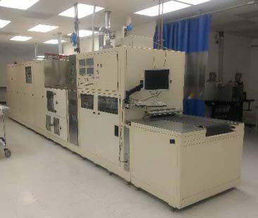
Watkins-Johnson WJ 16CVD250 APCVD System
The Watkins-Johnson WJ 16CVD250 APCVD System is a high-throughput atmospheric pressure chemical vapor deposition (APCVD) tool designed for depositing high-quality silicon dioxide (SiO2) thin films on large-area substrates. These systems have been widely used in semiconductor manufacturing, flat panel display production, AMLCD fabrication, and field emission display (FED) processing where uniform dielectric coatings are essential.
UniversityWafer, Inc. occasionally assists customers in locating quality pre-owned semiconductor equipment for research laboratories, pilot production, and manufacturing facilities. This listing is an example of available equipment that may be suitable for organizations expanding their thin-film deposition capabilities while reducing capital equipment costs.
Available Equipment
An end user is offering two Watkins-Johnson WJ 16CVD250 APCVD systems. Both systems were purchased new from the original manufacturer.
- One system is fully installed and operational.
- One system remains factory crated and was tested by Watkins-Johnson prior to shipment.
- Designed for large-area SiO2 deposition on substrates up to 400 mm × 500 mm.
- Installed system has been modified to operate two SnO2 deposition injectors.
- Includes spare injectors, vent assemblies, spare electronic boards, and chemical cabinet.
Typical Applications
The WJ 16CVD250 system is commonly used for depositing dielectric and transparent conductive films used in:
- Silicon dioxide (SiO2) thin-film deposition
- AMLCD manufacturing
- Field emission display (FED) fabrication
- Semiconductor wafer processing
- Glass substrate coating
- Research and pilot production facilities
System Specifications
- Model: Watkins-Johnson WJ 16CVD250 APCVD
- Deposition Area: Up to 400 × 500 mm substrates
- Belt Width: 18 inches
- Injectors Included: Three 16-inch injectors
- Vent Assemblies: Included
- Support Equipment: Spare boards and chemical cabinet included
Film Performance
- Within-wafer thickness uniformity: < ±5%
- Wafer-to-wafer thickness uniformity: < ±5%
- Refractive Index: 1.45 ± 0.02
- Wet Etch Rate: Approximately 500 Å/min
- Film Stress: < 2 × 10⁶ dynes/cm²
- Particle Density: <10 particles/cm² (>0.3 μm)
- Dielectric Breakdown: >8 MV/cm
- Dielectric Constant: Approximately 4.0–4.5
Production Throughput
- 400 × 300 mm substrates: 88+ plates/hour
- 370 × 470 mm substrates: 57+ plates/hour
- 400 × 500 mm substrates: 53+ plates/hour
- Guaranteed utilization: Greater than 80%
Process Gas Requirements
- Nitrogen: 425 lpm @ 44–55 PSIG
- Purge/Dilution Nitrogen: 28 lpm @ 25–35 PSIG
- 100% Silane: 200 sccm @ 25–35 PSIG
- Oxygen: 30 lpm @ 25–35 PSIG
Equipment Availability
The equipment became available because the manufacturing facility transitioned to a different production process. Originally offered individually, both APCVD systems, along with the spare components, are now available together for organizations seeking high-capacity semiconductor deposition equipment.
Listing ID: 9186673
Interested in Semiconductor Equipment? Contact UniversityWafer, Inc. for current availability, pricing, additional specifications, or assistance locating CVD systems, diffusion furnaces, wafer processing equipment, and semiconductor manufacturing tools.