
Looking for possibly more of these silicon wafers: Item #478. We use them as sputtering process witness coupons and are looking for the most affordable option that can be diced into small coupons. We would like pricing for approximately 250 pieces and recommendations for alternative substrates if available.
Silicon Witness Coupons for Sputtering Processes
Silicon witness coupons are commonly used during sputtering and thin film deposition processes to monitor coating thickness, film uniformity, contamination levels, adhesion, and overall process consistency. Many manufacturers choose low-cost silicon wafers that can be diced into smaller coupons, providing an economical solution for process qualification and quality control.
Witness coupons are frequently analyzed using profilometry, ellipsometry, AFM, SEM, and other characterization techniques to verify deposition performance. Common applications include semiconductor manufacturing, MEMS fabrication, optical coatings, and research involving metal, dielectric, and oxide thin films.
A manufacturing manager requested a quote for the following:
Reference #321571 for specifications and pricing.
Sputtering Targets and Thin Film Deposition Services
Sputtering targets are critical components in physical vapor deposition (PVD) systems used to deposit thin films onto substrates such as silicon wafers, sapphire wafers, glass substrates, quartz, and other semiconductor materials. Target materials may include metals, alloys, oxides, nitrides, and magnetic materials depending on the desired coating properties.
Researchers utilize sputtering to create conductive layers, dielectric coatings, optical films, magnetic films, and protective surface coatings for semiconductor devices, sensors, MEMS structures, solar cells, and advanced electronics.
Below is an example of a sputtering target request:
Please quote the prices for the following sputtering target:
Material: SmCo5
Purity: 99.9%
Dimensions: 75 mm × 3 mm
Quantity: 1 Piece
Reference #271390 for pricing.
Get Your Sputtering Quote FAST! Or, Buy Online and Start Researching Today!
What Are Sputtered Films?
Sputtered films are thin layers of material deposited onto a substrate using a physical vapor deposition (PVD) technique known as sputtering. During the process, ions generated in a plasma strike a target material, ejecting atoms that travel through a vacuum chamber and deposit onto a substrate surface. Sputtered films are widely used in semiconductor manufacturing, optics, MEMS fabrication, sensors, and advanced materials research.
 Researchers commonly deposit sputtered films onto silicon wafers, sapphire substrates, glass wafers, quartz, silicon carbide, and other advanced materials. The resulting coatings provide excellent uniformity, adhesion, and reproducibility for both research and production environments.
How the Sputtering Process Works
Sputtering begins by introducing an inert gas, typically argon, into a vacuum chamber. A plasma is generated, and positively charged ions accelerate toward the sputtering target. When the ions strike the target surface, atoms are ejected and deposited onto the substrate, forming a thin film.
This process allows precise control over film thickness, composition, and uniformity, making sputtering one of the most widely used thin film deposition methods in the semiconductor industry.
Types of Sputtered Films
Several categories of sputtered films are commonly used in research and manufacturing:
- Metal Films – Copper (Cu), Aluminum (Al), Gold (Au), Platinum (Pt), Titanium (Ti), and Chromium (Cr).
- Dielectric Films – Silicon dioxide (SiO₂), silicon nitride (Si₃N₄), aluminum oxide (Al₂O₃), and hafnium oxide (HfO₂).
- Semiconductor Films – Zinc oxide (ZnO), indium tin oxide (ITO), gallium nitride (GaN), and silicon-based materials.
- Multilayer Films – Engineered stacks designed for optical coatings, MEMS devices, and advanced electronics.
- Protective Coatings – Wear-resistant and corrosion-resistant thin films.
Common Applications of Sputtered Films
Sputtered thin films are used throughout numerous industries:
- Semiconductor Manufacturing
- Microelectronics and Integrated Circuits
- MEMS Devices
- Solar Cells and Photovoltaics
- Optical Filters and Mirrors
- Thin Film Sensors
- Medical Devices
- Display Technologies
- Aerospace Components
Many researchers use sputtered coatings to improve electrical conductivity, optical performance, chemical resistance, and surface durability.
Silicon Wafers for Sputtering Applications
Silicon wafers are among the most popular substrates for sputtered film deposition. Their excellent flatness, thermal stability, and compatibility with semiconductor processes make them ideal for research and production applications.
Silicon witness wafers and witness coupons are frequently used to monitor coating thickness, film uniformity, contamination levels, and process consistency during sputtering operations.
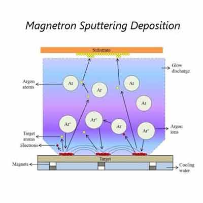
Magnetron Sputtering Deposition
Magnetron sputtering is one of the most common sputtering techniques used today. Magnets positioned behind the target confine electrons near the target surface, increasing plasma density and improving deposition efficiency.
Benefits of magnetron sputtering include:
- Higher deposition rates
- Improved film uniformity
- Lower substrate temperatures
- Excellent process repeatability
- Scalability for production environments
Reactive Sputtering
Reactive sputtering introduces gases such as oxygen or nitrogen into the vacuum chamber during deposition. These gases react with the sputtered material to form compound thin films including oxides, nitrides, and other functional coatings.
Reactive sputtering is commonly used to produce:
- Silicon Nitride (Si₃N₄)
- Titanium Nitride (TiN)
- Aluminum Oxide (Al₂O₃)
- Zinc Oxide (ZnO)
- Hafnium Oxide (HfO₂)
Advantages of Sputtered Thin Films
Sputtered coatings offer several advantages compared to other deposition techniques:
- Excellent adhesion to substrates
- High film density
- Superior thickness control
- Uniform coatings across large wafer surfaces
- Ability to deposit metals, oxides, nitrides, and alloys
- Excellent repeatability for research and production
Substrates Commonly Used for Sputtered Films
Sputtered coatings can be deposited on a wide range of substrates, including:
- Silicon Wafers
- Sapphire Wafers
- Glass Substrates
- Fused Silica Wafers
- Quartz Wafers
- Silicon Carbide Substrates
Choosing the proper substrate depends on electrical, optical, thermal, and mechanical requirements for the final device.
Why Researchers Use Sputtered Films
Sputtered films provide precise control over material properties and film thickness, making them essential for semiconductor fabrication, optics, MEMS devices, advanced sensors, and nanotechnology research. Their versatility and repeatability continue to make sputtering one of the most important thin film deposition technologies used today.
Video: Learn About Sputtered Thin Films