
Where Can You Buy Silicon Wafers?
UniversityWafer supplies silicon wafers for semiconductor research, microfabrication, MEMS, photonics, thin-film deposition, university laboratories, and production applications. Wafers are available in a wide range of diameters, crystal orientations, resistivities, thicknesses, dopants, grades, and surface finishes.
Whether you need a small quantity for research or larger quantities for process development and production, provide your required specifications and quantity using the form below. Our team can help identify a suitable silicon substrate for your application.
Get Your Silicon Wafer Quote FAST! Or, Buy Online and start researching today!
How Are Silicon Wafers Manufactured?
Silicon wafers begin as high-purity silicon that is converted into a single-crystal ingot and then sliced, processed, polished, and cleaned. Each manufacturing step helps control the wafer's crystal quality, dimensions, flatness, and surface condition for semiconductor fabrication and research.
-
Silicon Purification: Silicon is refined to achieve the high purity required for semiconductor applications. High-purity material is essential because unwanted impurities can affect the electrical properties of the finished substrate.
-
Single-Crystal Growth: High-purity silicon can be grown into a single-crystal ingot using the Czochralski (CZ) process . A seed crystal establishes the desired crystal orientation as the silicon ingot is formed.
-
Ingot Shaping and Slicing: The cylindrical silicon ingot is shaped to the required diameter and sliced into individual wafers. Precision slicing allows manufacturers to control wafer thickness while minimizing material loss.
-
Edge Grinding and Surface Preparation: After slicing, wafer edges are shaped and the surfaces may undergo grinding, lapping, or etching to remove slicing damage and improve dimensional uniformity.
-
Wafer Polishing: For applications requiring a highly smooth surface, chemical-mechanical polishing (CMP) is used to create a mirror-like finish suitable for photolithography, deposition, and other semiconductor processes.
-
Cleaning and Inspection: Finished wafers are cleaned to remove particles and surface contaminants and can be inspected for characteristics such as thickness, flatness, surface quality, crystal orientation, and other required specifications.
What Specifications Should You Provide?
When requesting a silicon wafer quote, providing the main substrate specifications helps identify the correct wafer more quickly. Important requirements may include:
- Diameter: such as 50.8mm, 76.2mm, 100mm, 150mm, 200mm, or 300mm
- Crystal Orientation: (100), (110), or (111)
- Conductivity Type: P-type, N-type, or undoped
- Dopant: such as boron, phosphorus, arsenic, or antimony
- Resistivity: specified in ohm-cm (Ω·cm)
- Thickness: standard or custom thickness requirements
- Surface Finish: SSP, DSP, lapped, or other required finish
- Grade: Prime, Test, Mechanical/Dummy, or another required grade
- Quantity: number of wafers required
Don't know every specification? Tell us about your process or application in the quote form and UniversityWafer can help determine suitable options.
What Are Silicon Wafers?
Silicon wafers are thin, circular slices of high-purity crystalline silicon used as the foundation for semiconductor devices, integrated circuits, sensors, MEMS, photonic components, and many other electronic technologies. They provide the flat, stable surface required for processes such as photolithography, oxidation, thin-film deposition, doping, etching, and metallization.
Most silicon wafers are produced from single-crystal silicon ingots grown using the Czochralski (CZ) or Float Zone (FZ) process. The ingot is sliced into wafers, ground, polished, and cleaned to achieve the surface quality and dimensional tolerances required for semiconductor processing.
Silicon wafers are available in different diameters, crystal orientations, conductivity types, resistivities, thicknesses, and surface finishes. These specifications are selected according to the electrical, mechanical, optical, or fabrication requirements of the intended application.
What Are Silicon Wafers Used For?
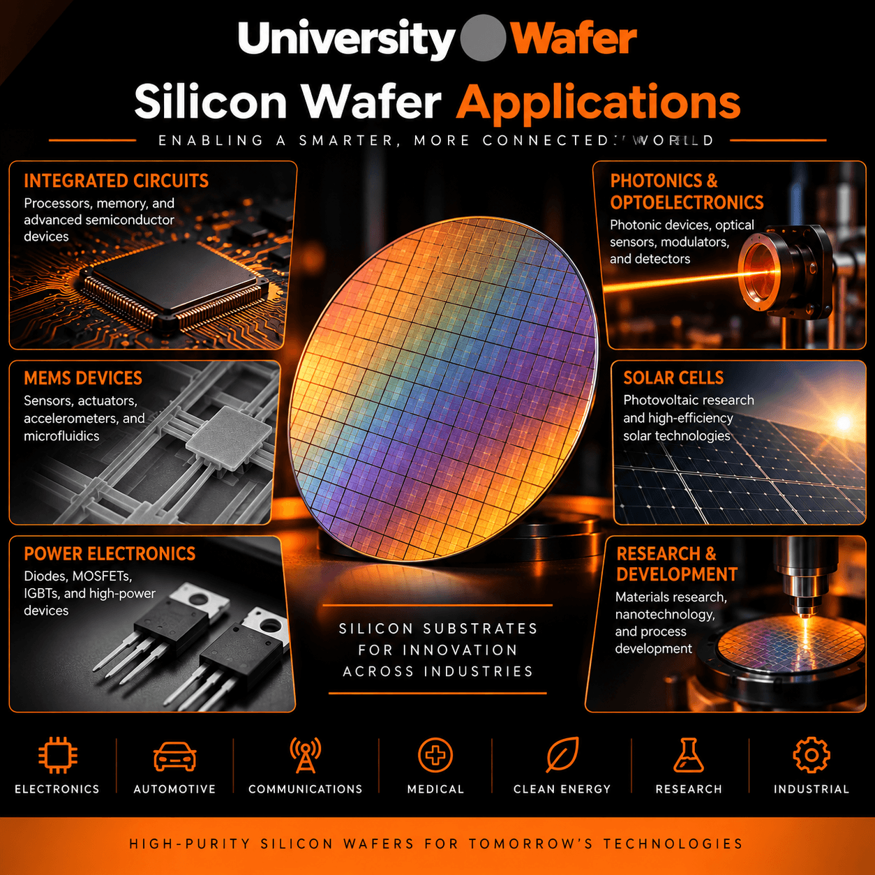
Silicon wafers are used across semiconductor manufacturing, microfabrication, electronics, energy research, and materials science. Some of the most common applications include:
- Integrated Circuits and Microchips: Silicon wafers are used as the starting substrate for transistors, processors, memory devices, and integrated circuits used in computers, smartphones, and electronic systems.
- MEMS Devices: Silicon is widely used for microelectromechanical systems such as accelerometers, pressure sensors, gyroscopes, microphones, and microfluidic structures.
- Power Electronics: Silicon substrates are used in diodes, MOSFETs, thyristors, and other components used for switching and controlling electrical power.
- Photonics and Optoelectronics: Silicon wafers are used in silicon photonics, optical sensors, modulators, detectors, and other devices that combine electronic and optical functions.
- Solar Cell Research: Crystalline silicon wafers are commonly used as the active substrate in photovoltaic devices and solar cell development.
- Nanotechnology and Materials Research: Silicon and silicon dioxide surfaces are frequently used for thin-film growth, graphene, 2D materials, nanostructures, and surface characterization.
- Process Development and Equipment Testing: Test and mechanical-grade silicon wafers are often used for deposition trials, furnace loading, dicing tests, lithography setup, and process calibration.
How Are Silicon Wafers Manufactured?
The manufacturing process begins with high-purity silicon, which is melted and grown into a single-crystal ingot. The ingot is then sliced into thin wafers and processed to achieve the required thickness, flatness, and surface finish.
- Silicon Purification: Raw silicon is refined to reach the purity levels required for semiconductor applications.
- Crystal Growth: A single-crystal silicon ingot is grown using methods such as the Czochralski or Float Zone process.
- Ingot Slicing: The silicon ingot is sliced into individual wafers using precision wire-saw or cutting systems.
- Edge Grinding and Lapping: The wafer edges and surfaces are processed to improve flatness, thickness uniformity, and mechanical integrity.
- Polishing: Chemical-mechanical polishing creates the smooth, mirror-like surface required for many semiconductor fabrication processes.
- Cleaning and Inspection: Wafers are cleaned and inspected for particles, surface defects, thickness, flatness, and other specifications.
Important Silicon Wafer Specifications
The performance of a silicon wafer depends on several key specifications. Selecting the correct combination is important for reliable fabrication and research results.
- Diameter: Common wafer diameters include 25.4mm, 50.8mm, 76.2mm, 100mm, 150mm, 200mm, and 300mm.
- Crystal Orientation: Common orientations include (100), (110), and (111).
- Conductivity Type: Silicon wafers may be P-type, N-type, or undoped.
- Dopant: Common dopants include boron for P-type silicon and phosphorus, arsenic, or antimony for N-type silicon.
- Resistivity: Resistivity affects electrical conductivity and is selected according to the device or research requirement.
- Thickness: Wafer thickness varies by diameter and application, with both standard and custom thicknesses available.
- Surface Finish: Wafers may be single-side polished (SSP), double-side polished (DSP), lapped, etched, or otherwise processed depending on the application.
Why Is Silicon Used for Semiconductor Wafers?
Silicon is widely used because it combines useful semiconductor electrical properties with mechanical strength, thermal stability, mature processing technology, and the ability to form a high-quality native oxide. These characteristics make it well suited for integrated circuits, MEMS, sensors, power devices, and many other semiconductor applications.
Buy Silicon Wafers for Research and Production
UniversityWafer supplies silicon wafers in a wide range of diameters, orientations, resistivities, dopants, thicknesses, grades, and surface finishes for research, prototyping, and production.
Related Silicon Wafer Resources
- Silicon Wafers – Browse silicon wafers by diameter, grade, orientation, resistivity, dopant, thickness, and surface finish.
- Types of Silicon Wafers – Learn about different silicon wafer grades, specifications, and substrate options.
- Silicon Wafer Applications – Explore how silicon wafers are used in semiconductors, MEMS, photonics, sensors, and research.
- Silicon Wafer Crystal Orientation – Compare (100), (110), and (111) silicon orientations and their applications.
- Silicon Wafer Resistivity – Understand how doping and resistivity affect the electrical properties of silicon substrates.
- Czochralski Silicon Crystal Growth – Learn how single-crystal silicon ingots are grown before being sliced into wafers.
- How Silicon Wafers Become Computer Chips – Follow the semiconductor fabrication steps used to transform silicon wafers into integrated circuits.