
Understanding the MOCVD Process
Metal-Organic Chemical Vapor Deposition (MOCVD) is an epitaxial growth technique used to deposit precisely controlled crystalline semiconductor layers onto a substrate. The process is especially important for III-V and III-N compound semiconductors used in optoelectronics, RF electronics, power devices, photonics, and advanced semiconductor research.
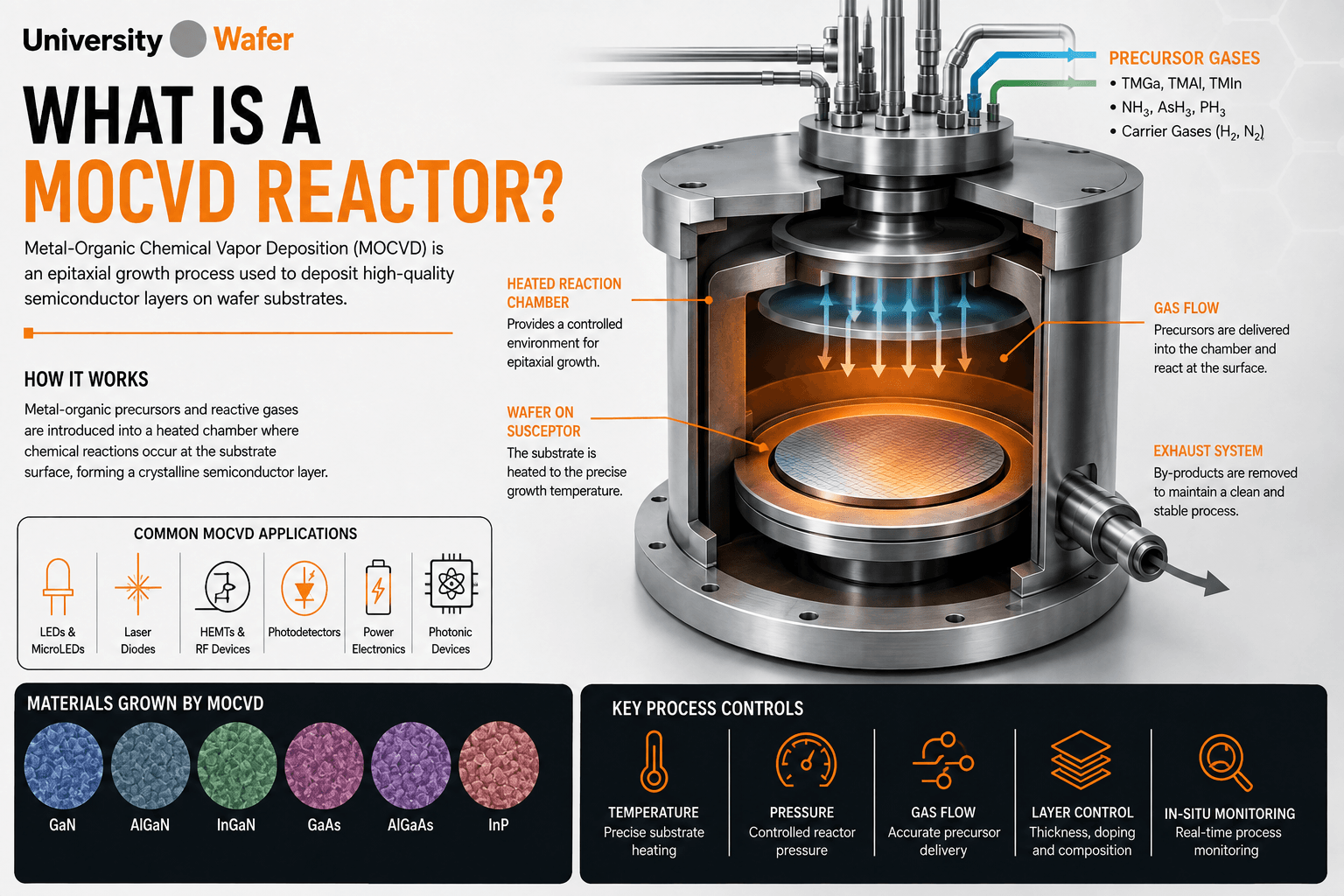
Inside a MOCVD reactor, carefully controlled precursor gases are transported into a reaction chamber containing heated wafer substrates. Chemical reactions occur at or near the substrate surface, allowing crystalline layers to grow while researchers control properties such as composition, thickness, doping, and heterostructure design.
Main Components of a MOCVD Reactor
Although reactor designs vary, a MOCVD system generally contains several major components that work together to control epitaxial growth.
- Reaction chamber: Provides the controlled environment where epitaxial deposition occurs.
- Wafer susceptor: Holds the substrate and helps maintain the required growth temperature.
- Precursor delivery system: Introduces controlled quantities of metal-organic source materials into the reactor.
- Carrier and reactive gas lines: Transport process gases into the growth chamber.
- Temperature control: Maintains the substrate conditions required for chemical reactions and crystal growth.
- Pressure control: Regulates reactor pressure during deposition.
- Exhaust system: Removes reaction byproducts and unused process gases from the chamber.
How MOCVD Epitaxial Growth Works
During MOCVD growth, the wafer is heated while precursor and reactive gases flow through the reactor. Under the appropriate temperature and pressure conditions, precursor molecules decompose and react, allowing the desired semiconductor material to form on the crystalline substrate.
By changing precursor flow rates and process conditions during growth, researchers can create multilayer semiconductor structures with controlled compositions and interfaces. This capability makes MOCVD particularly useful for producing heterostructures and epitaxial layers for advanced electronic and optoelectronic devices.
Semiconductor Materials Grown by MOCVD
MOCVD is commonly associated with compound semiconductor materials and heterostructures, including:
- Gallium Nitride (GaN)
- Aluminum Gallium Nitride (AlGaN)
- Indium Gallium Nitride (InGaN)
- Gallium Arsenide (GaAs)
- Aluminum Gallium Arsenide (AlGaAs)
- Indium Phosphide (InP)
- Related III-V and III-N semiconductor structures
Why Substrate Selection Matters
The substrate provides the crystalline foundation for epitaxial growth. Its material, crystal orientation, surface condition, diameter, lattice properties, and thermal characteristics can influence the quality of the resulting epitaxial structure.
Depending on the semiconductor system being investigated, MOCVD research may use sapphire, silicon carbide (SiC), silicon, gallium arsenide (GaAs), indium phosphide (InP), or existing epitaxial templates.
MOCVD Applications
The ability to control semiconductor layer composition and thickness makes MOCVD valuable for research and fabrication involving:
- LEDs and microLEDs
- Laser diodes
- High-electron-mobility transistors (HEMTs)
- RF and microwave electronics
- Power semiconductor devices
- Photodetectors
- Photonic devices
- Compound semiconductor heterostructures
- Advanced epitaxial materials research
Substrates for MOCVD Research
UniversityWafer supplies research-grade substrates and epitaxial templates for MOCVD process development, semiconductor research, and device fabrication. Researchers can request wafers based on substrate material, diameter, orientation, surface finish, doping, epitaxial structure, and other project requirements.
Get Your MOCVD Research Wafer Quote FAST! Or, buy online and start researching today!
MOCVD Reactor Design and Growth Parameters
A MOCVD reactor must precisely control gas flow, substrate temperature, chamber pressure, precursor concentration, and wafer positioning. These variables influence epitaxial growth rate, composition, doping, surface morphology, thickness uniformity, and crystal quality.
Modern MOCVD systems combine a reaction chamber with high-purity gas delivery, wafer heating, pressure regulation, exhaust handling, and process-monitoring equipment to create repeatable conditions for compound semiconductor growth.
Common Types of MOCVD Reactors
MOCVD reactors can use different chamber and gas-flow configurations depending on wafer size, material system, throughput, and uniformity requirements.
Horizontal MOCVD Reactors
In a horizontal reactor, process gases generally flow across the heated substrate. These systems are commonly used for research and epitaxial process development because the gas flow and wafer environment can be carefully controlled.
Vertical MOCVD Reactors
Vertical reactors direct precursor gases toward wafers using a vertical flow configuration. Reactor geometry and gas distribution are engineered to promote uniform precursor delivery across the substrate surface.
Showerhead Reactors
A showerhead configuration distributes process gases through multiple openings positioned above the wafer region. The design helps provide controlled precursor distribution across the substrate and is useful when uniform epitaxial growth over larger wafer areas is required.
Planetary MOCVD Reactors
Planetary systems can rotate multiple wafers during deposition. Wafer rotation and controlled gas flow help improve growth uniformity and make this configuration useful for higher-throughput epitaxial processing.
MOCVD Precursors and Carrier Gases
MOCVD relies on volatile chemical precursors to supply the elements required for crystal growth. The exact chemistry depends on the semiconductor material being deposited.
Common group-III metal-organic precursors include:
- TMGa – Trimethylgallium for gallium
- TMAl – Trimethylaluminum for aluminum
- TMIn – Trimethylindium for indium
Common group-V source gases include:
- NH3 – Ammonia for nitrogen
- AsH3 – Arsine for arsenic
- PH3 – Phosphine for phosphorus
Carrier gases transport the precursor species through the reactor toward the heated substrate. Hydrogen and nitrogen are commonly used depending on the material system and growth process.
Temperature Control
Substrate temperature is one of the most important MOCVD process variables. The wafer is typically positioned on a heated susceptor, which provides controlled thermal conditions during epitaxial growth.
Temperature affects precursor decomposition, surface reactions, atomic mobility, growth rate, composition, and crystal quality. Maintaining uniform temperature across the wafer is therefore important for obtaining consistent epitaxial layers.
Reactor Pressure and Gas Flow
MOCVD growth is performed under carefully controlled reactor pressure and gas-flow conditions. Mass-flow controllers can regulate individual process gases, allowing researchers to adjust precursor ratios and growth conditions for different epitaxial layers.
Precise gas delivery becomes especially important when producing multilayer structures where composition or doping must change from one layer to another.
Controlling Epitaxial Layer Composition
One of the major advantages of MOCVD is the ability to change precursor concentrations during growth. This allows researchers to fabricate complex semiconductor heterostructures rather than depositing only a single material.
Examples include:
- GaN / AlGaN heterostructures
- InGaN / GaN multiple quantum wells
- GaAs / AlGaAs structures
- InP / InGaAsP structures
- AlN / AlGaN / GaN buffer systems
These structures can be engineered by controlling layer thickness, alloy composition, doping, and interfaces during the growth sequence.
Doping During MOCVD Growth
Controlled doping can be incorporated during epitaxial growth to modify the electrical properties of semiconductor layers. Dopant sources are introduced in carefully controlled concentrations along with the primary growth precursors.
For example, silicon-containing sources may be used for n-type doping in certain material systems, while magnesium-containing precursors such as Cp2Mg are commonly associated with p-type doping of GaN-based materials.
Why Epi-Ready Wafers Matter
The MOCVD reactor cannot compensate for every defect or contaminant present on the starting substrate. Epi-ready wafers are precision-polished and prepared specifically for epitaxial deposition, helping provide a clean, smooth, and controlled starting surface.
Important substrate specifications may include:
- Crystal orientation
- Wafer diameter and thickness
- Surface roughness
- Epi-ready surface finish
- Miscut or off-axis orientation
- Total thickness variation (TTV)
- Wafer bow and warp
- Substrate doping and resistivity
UniversityWafer offers epi-ready silicon, sapphire, GaAs, GaN, SiC, InP, germanium, and other semiconductor substrates for MOCVD, MBE, and related epitaxial growth research.
MOCVD Process Monitoring
Advanced MOCVD systems may incorporate in-situ monitoring methods such as reflectometry, pyrometry, and interferometry. These techniques can help researchers monitor parameters such as substrate temperature, reflectance, growth behavior, and layer development while deposition is taking place.
Evaluating MOCVD-Grown Layers
After growth, epitaxial wafers can be characterized using several semiconductor metrology techniques. The appropriate method depends on the material system and device requirements.
- AFM – evaluates surface morphology and roughness
- XRD / HRXRD – evaluates crystal structure, composition and strain
- Photoluminescence (PL) – evaluates optical properties and emission behavior
- SEM / TEM – examines surface features, interfaces and defects
- Hall measurements – evaluates carrier concentration and mobility
MOCVD for Research and Semiconductor Development
MOCVD combines precise chemical delivery with controlled temperature and pressure to produce sophisticated epitaxial semiconductor structures. Its ability to grow uniform III-V and III-N layers makes it important for developing LEDs, microLEDs, lasers, HEMTs, RF devices, photodetectors, photonics, and power electronics.
Selecting the correct substrate, surface finish, crystal orientation, and wafer geometry provides the foundation needed for repeatable MOCVD growth and reliable semiconductor research.