
Semiconductor Wafers
We have a large selection of substrates used to fabricate 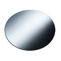 semiconductors. Pelase fill out the form below with your specs and quantity for an immediate quote.
Get Your Quote FAST! Or, Buy Online and Start Your Research Today!
What is a Wafer and Why Should You Care?
A wafer is a thin, circular disc made of a semiconductor material, such as silicon, that is used as the substrate (base material) for the fabrication of microelectronic devices, such as microprocessors, memory chips, and other integrated circuits. Wafers are typically a few hundred micrometers thick and can range in diameter from a few millimeters to a few inches.
Wafers are produced through a process called wafer manufacturing, in which a single crystal of silicon or other semiconductor material is grown, sliced into thin discs, ground and polished to remove defects, and cleaned to remove contaminants. The resulting wafers are high-purity, high-quality discs that are ready for the next steps in the microelectronic device manufacturing process.
Wafers are used as the starting material for the fabrication of microelectronic devices because they provide a flat, smooth, and uniform surface on which to build the various layers and components of the device. They are also highly conductive and have excellent electrical and thermal properties, which are important for the performance of the device. Wafers are used in a variety of applications, including computing, telecommunications, and consumer electronics, and are an essential component of modern microelectronic devices.
Silicon is a chemical element with the atomic number 14 and the symbol Si. It is a member of the group 14 of the periodic table, which also includes carbon and germanium, and is the second most abundant element in the Earth's crust, after oxygen.
What are Silicon Wafers So Important?
Silicon wafers are important to semiconductor devices because it is an excellent semiconductor material, meaning that it can conduct electricity under certain conditions and can also act as an insulator under other conditions. This property makes it ideal for use in the construction of microelectronic devices, such as microprocessors, memory chips, and other integrated circuits, which rely on the controlled flow of electricity to perform their functions.
Silicon has a number of other properties that make it particularly useful for semiconductor applications, including:
-
High melting point: Silicon has a high melting point of 1414 °C, which makes it resistant to thermal degradation and allows it to withstand high temperatures during the manufacturing process.
-
High thermal conductivity: Silicon has a high thermal conductivity, which makes it an efficient heat sink and helps to dissipate heat generated by the device.
-
High chemical stability: Silicon is highly resistant to chemical attack and is not reactive with most other elements, making it a stable and reliable material for use in microelectronic devices.
-
Abundance: Silicon is the second most abundant element in the Earth's crust, making it a readily available and inexpensive material for use in microelectronic devices.
Due to its excellent properties and wide availability, silicon is the most commonly used material for the construction of microelectronic devices and is an essential component of modern electronics.