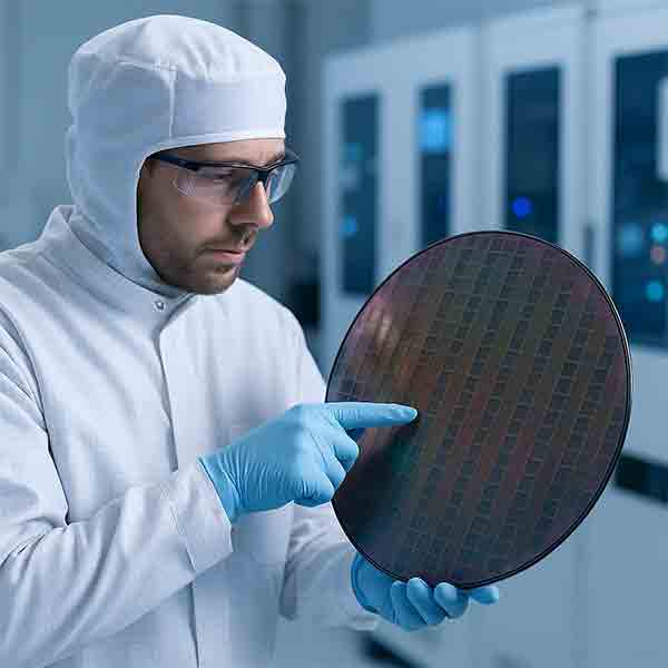
Semiconductor Yield Engineer: Improving Wafer Yield and Process Performance 

Semiconductor yield engineers use wafer test data, defect inspection, wafer maps, metrology, and statistical process control (SPC) to identify sources of yield loss and improve manufacturing performance. Explore how defect density, process variation, equipment conditions, and substrate quality can influence die yield and semiconductor process optimization.

UW Logo

Understanding Semiconductor Wafer Yield

In semiconductor manufacturing, yield describes the fraction of fabricated devices that meet the required electrical, functional, and reliability specifications. High yield is essential for efficient production, but achieving it requires tight control of materials, equipment, and hundreds of individual fabrication steps.

Yield loss can result from random defects, systematic process problems, equipment excursions, contamination, dimensional variation, or interactions between device design and fabrication processes. Yield engineers use manufacturing and test data to identify these sources and determine which improvements will have the greatest impact.

What Can Reduce Semiconductor Yield?

A semiconductor wafer passes through many processes before individual dies are tested. Variation or defects introduced during any critical step can reduce final device yield.

Particle and Surface Contamination

Particles, metallic contamination, organic residues, and other unwanted material can interfere with lithography, deposition, etching, oxidation, interfaces, and electrical structures. Whether a particular defect causes device failure depends on its size, location, and interaction with critical device features.

Lithography and Patterning Variation

Semiconductor lithography requires accurate control of critical dimensions, focus, exposure, resist processing, and layer-to-layer overlay. Patterning errors can produce opens, shorts, malformed features, or dimensional deviations that affect device performance.

Thin-Film and Etch Non-Uniformity

Variations in deposited film thickness, composition, stress, or etch depth can produce electrical and structural differences across a wafer. Monitoring wafer-level uniformity helps engineers determine whether variation remains within the allowable process window.

Process Equipment Variation

Differences between tools, chambers, recipes, or processing conditions can create measurable changes in device performance. Comparing yield and metrology data by equipment history can help identify systematic sources of variation.

Starting Wafer Characteristics

The substrate itself is another important process variable. Depending on the device and process, relevant wafer specifications can include crystal orientation, resistivity, conductivity type, thickness, total thickness variation (TTV), bow, warp, surface condition, crystal defects, and oxide or epitaxial-layer properties.

Wafer Maps Help Reveal Yield Problems

After wafer-level electrical testing, results can be displayed as a wafer map showing where passing and failing dies are located. Spatial failure patterns can provide valuable clues about the underlying manufacturing problem.

For example, engineers may investigate edge-related failures, localized clusters, repeating patterns, scratches, or other non-random distributions. These patterns can then be compared with inspection, metrology, equipment, and process-history data to identify possible root causes.

Random vs. Systematic Yield Loss

Yield loss is often analyzed by distinguishing between random defects and systematic failure mechanisms.

Random defects may arise from particles or other localized events that occur probabilistically across the wafer. Systematic yield loss can arise from repeatable process, equipment, layout, or integration problems and may produce recognizable patterns across dies, wafers, or lots.

Defect Density and Die Size

For random yield-limiting defects, larger dies generally have a greater probability of intersecting a critical defect because they occupy more wafer area. A simple Poisson defect model illustrates this relationship:

Y = e-D0A

where Y represents modeled die yield, D0 represents critical defect density, and A represents die area.

This equation is useful for illustrating defect-limited yield, but real semiconductor manufacturing is more complex. Defects may cluster spatially, and systematic failure mechanisms are not fully represented by a simple Poisson model.

From Wafer Data to Root Cause

Yield improvement typically requires combining information from multiple sources rather than relying on a single measurement. Engineers may correlate:

  • Electrical wafer-sort and parametric test results
  • Wafer maps and spatial failure patterns
  • Defect inspection and microscopy data
  • Film thickness and critical-dimension measurements
  • Overlay and lithography data
  • Equipment, chamber, and recipe histories
  • Lot-to-lot and wafer-to-wafer variation
  • Failure-analysis results

Correlating these datasets helps distinguish coincidence from repeatable relationships and supports evidence-based corrective action.

Yield Learning and Process Development

During development of a new semiconductor process or device, initial yield may be lower than the level required for economical volume manufacturing. Engineers progressively identify dominant failure mechanisms, improve process control, reduce defectivity, and verify corrective actions.

This iterative improvement is commonly called yield learning or yield ramp. Stable manufacturing requires not only high average yield but also consistent performance across wafers, lots, tools, and time.

Wafers for Semiconductor Process and Yield Research

UniversityWafer supplies semiconductor substrates for process development, equipment testing, materials research, characterization, and fabrication experiments. Researchers can select wafers based on parameters such as diameter, orientation, thickness, resistivity, conductivity type, surface finish, and oxide or epitaxial-layer requirements.

Using substrates with documented and consistent specifications can help researchers control starting-material variables when evaluating new fabrication processes or investigating sources of process variation.

Get Your Semiconductor Wafer Quote FAST! Or, Buy Online and Start Researching Today!


What Is a Semiconductor Yield Engineer?

A semiconductor yield engineer analyzes fabrication and test data to determine why some dies or wafers fail to meet specification and identifies opportunities to increase the percentage of functional devices produced by a manufacturing process.

In semiconductor manufacturing, yield is influenced by many factors, including particle contamination, lithography defects, film non-uniformity, process variation, equipment performance, material quality, device design, and interactions between individual fabrication steps.

Semiconductor yield engineer substrate applications for wafer map analysis, defect analysis, process control, equipment qualification, reliability testing, and yield ramp

How Do Yield Engineers Improve Wafer Yield?

Yield engineering combines semiconductor process knowledge with statistics, metrology, inspection, electrical test data, and failure analysis. Engineers look for patterns that connect failed devices to specific wafer locations, process steps, tools, materials, or manufacturing conditions.

Wafer Map and Test Data Analysis

Wafer maps show the spatial distribution of passing and failing dies across a wafer. Patterns such as edge failures, localized clusters, scratches, repeating signatures, or systematic regions of low yield can provide clues about the source of a manufacturing problem.

Defect Detection and Root-Cause Analysis

Optical inspection, electron-beam inspection, microscopy, electrical testing, and other characterization techniques can be used to identify defects and determine whether they are associated with a particular fabrication step. Not every detected defect causes device failure, so correlating defects with electrical and functional test results is an important part of yield analysis.

Statistical Process Control (SPC)

Yield engineers use statistical process control and other statistical methods to monitor critical process parameters and identify abnormal shifts or trends. Parameters may include film thickness, critical dimensions, overlay, etch depth, sheet resistance, defect density, and other measurements relevant to the process.

Process and Equipment Commonality

When yield changes, engineers may compare wafers, lots, recipes, chambers, and individual production tools to identify common factors associated with the failures. This type of analysis can help distinguish random defects from systematic equipment or process problems.

Why Does Defect Density Matter?

Defect density is an important factor in semiconductor yield because a critical defect within a device area can cause a die to fail. In a simple Poisson yield model, the relationship can be expressed as:

Y = e-D0A

where Y is the modeled die yield, D0 is the critical defect density, and A is the die area. The model illustrates why larger dies generally have a greater probability of encountering a random defect when defect density is held constant.

Real semiconductor processes can exhibit defect clustering and systematic failure mechanisms, so more sophisticated yield models may be required for accurate prediction and analysis.

Yield Engineering During Process Development

Yield engineering is especially important when a semiconductor process moves from development toward volume manufacturing. During yield ramp, engineers work to identify dominant failure mechanisms, reduce defectivity, stabilize process conditions, and improve manufacturing consistency.

This work is typically cross-functional. Yield engineers collaborate with process engineers, equipment engineers, integration teams, product engineers, failure-analysis specialists, test engineers, and device designers to isolate problems and verify corrective actions.

Why Wafer Quality Matters for Yield Engineering

Reliable experiments require well-characterized starting substrates. Properties such as wafer diameter, thickness, total thickness variation (TTV), surface finish, crystal orientation, resistivity, dopant type, oxide thickness, and defect levels can influence downstream processing and experimental results.

Consistent substrate specifications help researchers distinguish variation introduced by the starting wafer from variation generated during deposition, lithography, etching, oxidation, epitaxy, implantation, annealing, and other fabrication processes.

Silicon Wafers and Coupons for Yield Research

UniversityWafer supplies silicon wafers, diced coupons, oxidized wafers, epitaxial substrates, SOI wafers, and other research substrates that can be used for process development, characterization, equipment qualification, defect studies, and semiconductor yield experiments.

Researchers can specify parameters such as diameter, thickness, orientation, resistivity, conductivity type, surface finish, oxide thickness, and other substrate requirements to support a particular experiment or fabrication process.

Related Semiconductor Yield & Wafer Resources