
Germanium Wafer Properties
Germanium (Ge) is a high-purity elemental semiconductor used in advanced electronic, optical, and materials research. Its combination of high carrier mobility, infrared transmission, and semiconductor properties makes germanium wafers useful for both fundamental research and device development.
Why Researchers Use Germanium
Germanium offers higher electron and hole mobility than conventional silicon, making it attractive for research into high-speed electronics, advanced transistors, photonics, and next-generation semiconductor devices.
- High carrier mobility for advanced electronic devices
- Infrared transparency for optical and detector research
- Semiconductor properties suitable for device fabrication
- III-V compatibility for selected epitaxial structures
- Photovoltaic applications including high-efficiency solar cell research
Germanium for Photonics and IR Research
The optical properties of germanium make it particularly valuable for infrared (IR) detectors, imaging, photonics, and optoelectronics. Researchers can use polished Ge substrates for thin-film deposition, optical characterization, and experimental device fabrication.
Ge Wafers for Solar Cell Research
Germanium substrates are also used in multijunction solar cell research, where they can support the growth of III-V semiconductor layers. These structures are investigated for high-efficiency photovoltaic technologies and other demanding optoelectronic applications.
Choosing a Germanium Substrate
Important specifications when selecting a Ge wafer include diameter, thickness, crystal orientation, conductivity type, resistivity, doping, and surface finish. Selecting the appropriate specifications helps ensure compatibility with your deposition, epitaxy, fabrication, or characterization process.
UniversityWafer can help researchers source germanium wafers with specifications suited to university, laboratory, semiconductor, and R&D applications.
Get Your Germanium Wafer Quote FAST! Or Buy Online and Start Researching Today!
Germanium Wafers for Advanced Research
Germanium (Ge) is an elemental semiconductor valued for its high carrier mobility, infrared transparency, and compatibility with advanced semiconductor processing. Germanium wafers are widely investigated for applications in photonics, infrared optics, high-speed electronics, detectors, and photovoltaic research.
Compared with conventional silicon wafers, germanium offers significantly higher electron and hole mobility. These properties make Ge an important material for researchers developing high-performance transistors and other next-generation semiconductor devices.
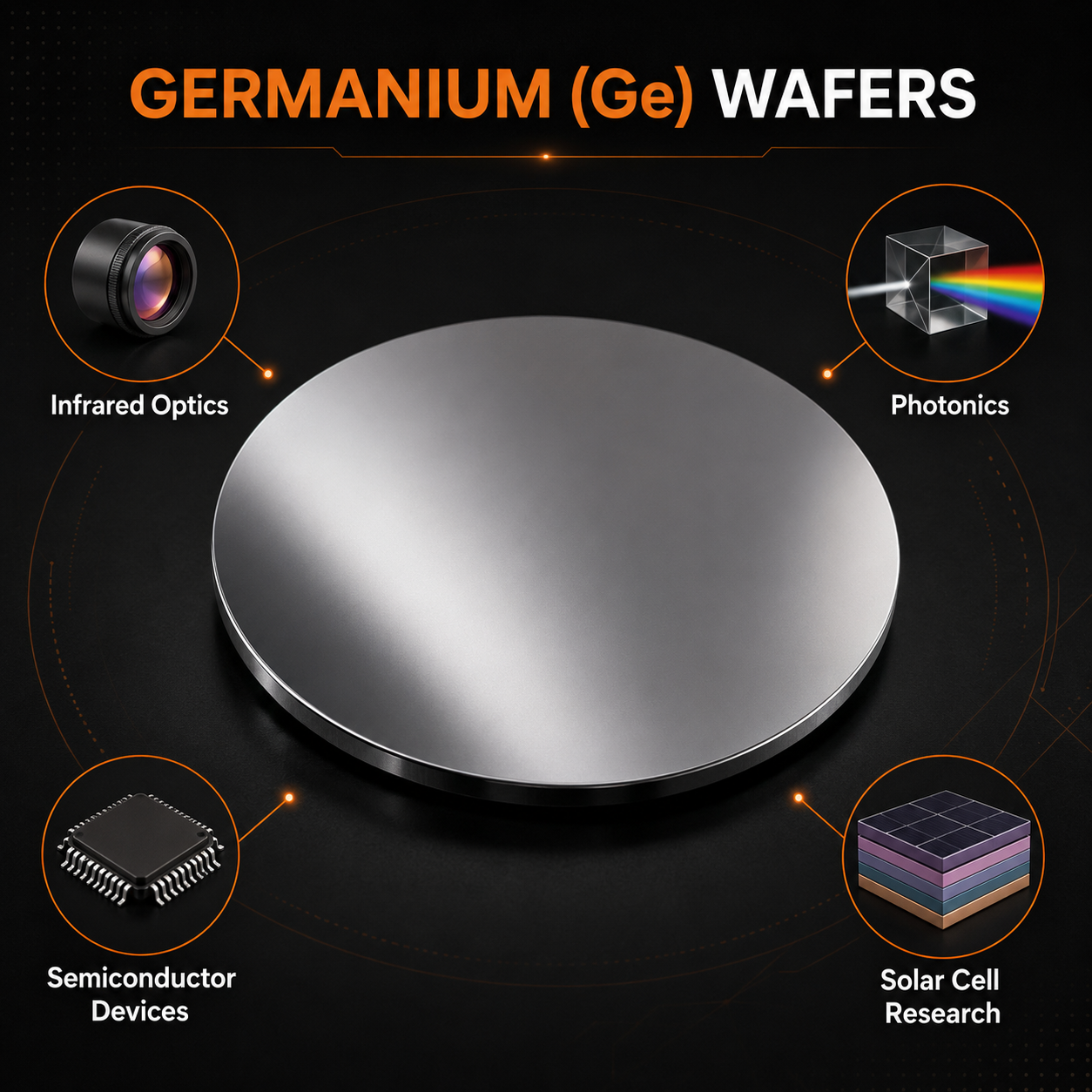
Germanium Wafer Applications
Germanium substrates can be used for research involving:
- Infrared (IR) optics and detectors
- Photonics and optoelectronics
- High-speed semiconductor devices
- Solar cells and photovoltaic research
- III-V semiconductor epitaxy
- Transistor and device fabrication
- Material science and thin-film research
Germanium for Infrared Applications
Germanium is especially useful for infrared research because of its optical properties in the infrared spectral region. Ge substrates can be incorporated into experimental IR detectors, optical components, imaging systems, and other photonic devices.
Germanium as a Semiconductor Substrate
The high carrier mobility of germanium continues to make it an important research material for advanced electronics. Researchers study Ge for high-speed transistors, CMOS technologies, heterostructures, and epitaxial growth.
Germanium can also serve as a substrate for selected III-V semiconductor materials, providing researchers with additional options when developing compound-semiconductor and optoelectronic structures.
Germanium Wafer Specifications
Depending on availability, germanium substrates may be supplied with different diameters, thicknesses, crystal orientations, conductivity types, doping levels, and surface finishes. Polished surfaces are available for applications requiring high-quality substrates for deposition, epitaxy, device fabrication, and characterization.
Contact UniversityWafer with your required germanium wafer specifications and research application so we can help identify an appropriate substrate.