
Zinc Selenide Wafers for Research
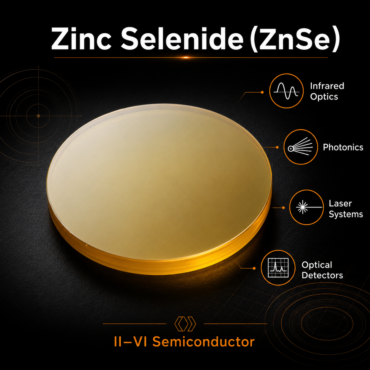
Zinc Selenide (ZnSe) is a II-VI compound semiconductor valued for its optical transparency and semiconductor properties. ZnSe substrates are used by researchers working in infrared optics, photonics, optoelectronics, laser technology, detectors, and thin-film development.
Why Use Zinc Selenide?
ZnSe combines useful optical and electronic characteristics, making it suitable for experiments involving light transmission, emission, detection, and semiconductor device development. Its properties make it particularly interesting for optical and infrared research.
- Infrared optics for optical and spectroscopy research
- Photonics and optoelectronic device development
- Laser research and optical components
- Detector applications for light and infrared sensing
- Thin-film deposition and coating studies
- II-VI semiconductor research and material characterization
ZnSe for Infrared and Optical Research
Zinc Selenide is widely investigated for infrared (IR) and optical applications. Researchers can use ZnSe substrates to study optical transmission, coatings, spectroscopy, photonic structures, and other experiments where interaction between semiconductor materials and light is important.
ZnSe for Thin-Film Research
Polished ZnSe substrates can also provide a useful surface for thin-film deposition and materials research. They may be used to investigate deposited semiconductor, dielectric, or optical layers and evaluate their structural, electrical, and optical characteristics.
Selecting a ZnSe Substrate
When selecting a Zinc Selenide substrate, researchers should consider specifications such as size, thickness, crystal orientation, surface finish, and material quality. The appropriate configuration will depend on the intended optical, deposition, characterization, or device-fabrication process.
UniversityWafer can help researchers source ZnSe substrates for university laboratories, semiconductor R&D, photonics, and advanced materials research.
Get Your Zinc Selenide Wafer Quote FAST! Or Buy Online and Start Researching Today!
Zinc Selenide (ZnSe) Properties and Applications
Zinc Selenide (ZnSe) is a II-VI compound semiconductor with optical and electronic properties that make it useful for infrared optics, photonics, lasers, detectors, and optoelectronic research. ZnSe substrates are particularly valuable when researchers need a material suitable for studying the interaction of light with semiconductor structures.
ZnSe for Infrared Optics
Zinc Selenide is widely used in infrared (IR) optical research. Its broad optical transmission range makes ZnSe useful for experimental windows, lenses, spectroscopy systems, and other optical components operating from visible wavelengths into the infrared.
Photonics and Optoelectronics Research
As a direct-bandgap II-VI semiconductor, ZnSe is studied for light-emitting, light-detecting, and photonic devices. Researchers can investigate ZnSe in optical structures, semiconductor heterostructures, detectors, and other next-generation optoelectronic technologies.
Common ZnSe Research Applications
- Infrared optics and spectroscopy
- Photonics and optoelectronic devices
- Laser components and optical systems
- IR and optical detectors
- Thin-film deposition and coatings
- II-VI semiconductor research
- Material characterization
ZnSe Substrates for Thin-Film Deposition
Polished ZnSe substrates can be used as starting surfaces for thin-film deposition, coating development, and materials characterization. Researchers can evaluate how deposited materials interact with the ZnSe surface and investigate their optical, structural, and electronic properties.
Choosing Zinc Selenide Substrates
Important factors when specifying a ZnSe substrate include dimensions, thickness, crystal orientation, surface finish, and material quality. Selecting the correct substrate specifications can improve compatibility with optical characterization, deposition, device fabrication, and other experimental processes.
UniversityWafer supplies semiconductor and research substrates for laboratories, universities, and R&D facilities developing advanced optical and electronic technologies.