
Custom AlN on Sapphire and AlN on Silicon Solutions
UniversityWafer supplies high-quality Aluminum Nitride (AlN) on sapphire wafers, AlN on Silicon substrates, and custom epitaxial templates for semiconductor research, UV LEDs, RF electronics, photonics, MEMS devices, and advanced materials science applications.
Our AlN templates are available with custom diameters, epitaxial layer thicknesses, surface roughness specifications, crystal orientations, and insulating substrate options for both research and production environments.
Recent AlN Wafer Research Request
A semiconductor researcher requested custom single-crystal Aluminum Nitride (AlN) grown on Silicon <111> substrates for advanced thin film and semiconductor applications.
The requested specifications included:
- 4-inch, 6-inch, or 8-inch wafers
- 1400nm AlN epitaxial layer
- 500nm PECVD SiO2 capping layer
- Single crystal AlN growth
- Prime grade silicon substrates
UniversityWafer provided quotes for both AlN on Silicon and AlN on Sapphire substrates with custom epitaxial layer structures optimized for semiconductor research and device fabrication.
Need Custom AlN Layer Thicknesses or PECVD Coatings? UniversityWafer can supply Aluminum Nitride wafers with custom epitaxial structures, oxide coatings, surface finishes, and substrate orientations.
Get Your AlN Wafer Quote FAST! Or, Buy Online and Start Researching Today!
AlN and GaN Templates for 2D Materials Research
Researchers working with 2D transition metal dichalcogenides (TMDCs), graphene, and advanced semiconductor thin films frequently request highly insulating GaN templates, AlN templates, and hBN substrates.
These templates are used to study epitaxial growth behavior, electrical properties, semiconductor interfaces, and thin film interactions while minimizing unwanted substrate conductivity effects.
Typical research specifications include:
- Single crystal epitaxial AlN and GaN layers
- High resistivity substrates (>106 ohm cm)
- Single-side polished sapphire substrates
- Custom polarity options
- 2-inch to 4-inch wafer diameters
- Low surface roughness for thin film growth
UniversityWafer supplies custom GaN templates, AlN templates, graphene substrates, and insulating semiconductor wafers for university research labs, photonics applications, and semiconductor fabrication studies.
Researchers studying 2D TMDC materials often investigate epitaxial growth on III-nitride substrates such as AlN and GaN to improve crystal quality, electrical performance, and device integration.
Recent AlN/Si Research Quote:
2-inch AlN on Silicon wafer, single crystal epitaxial AlN layer grown on Silicon substrate, single-side polished, high resistivity substrate (>106 ohm cm), Aluminum polar orientation, 25nm AlN layer.
Please contact UniversityWafer for pricing and availability. Reference #253427.
Aluminum Nitride on Sapphire Wafers
UniversityWafer, Inc. supplies high-quality Aluminum Nitride (AlN) on sapphire wafers and AlN on silicon substrates for semiconductor fabrication, UV LEDs, RF electronics, HEMT devices, photonics, MEMS, and advanced materials research.
Our AlN templates are available on c-plane sapphire and silicon substrates with custom diameters, AlN film thicknesses, orientations, surface roughness specifications, and epitaxial structures optimized for both research and production applications.

Applications of AlN on Sapphire
Aluminum Nitride on sapphire wafers are widely used in high-performance semiconductor and optoelectronic devices because of their excellent thermal conductivity, electrical insulation, wide bandgap properties, and compatibility with epitaxial semiconductor growth.
Common applications include:
- UV LED fabrication
- High-electron-mobility transistor (HEMT) templates
- RF filters and RF devices
- Piezoelectric devices
- Photonics and optoelectronics
- Power semiconductor devices
- MEMS fabrication
- 2D materials and TMDC research
- Laser and infrared sensor technologies
AlN-based UV LEDs are commonly used for sterilization, medical devices, water purification, and cleanroom disinfection because ultraviolet light can destroy bacteria and viruses without chemical treatments.
Advantages of Aluminum Nitride
Aluminum Nitride is a wide bandgap semiconductor material with exceptional thermal and electrical properties. Compared to conventional semiconductor materials, AlN offers:
- High thermal conductivity
- Excellent electrical insulation
- High breakdown voltage
- Low thermal expansion coefficient
- Strong chemical resistance
- High temperature stability
- Compatibility with UV optoelectronics
Because of these characteristics, AlN on sapphire is an important substrate material for next-generation semiconductor devices and high-frequency electronics.
AlN on Silicon Wafers
UniversityWafer also supplies AlN on Silicon wafers for thin film deposition, RF electronics, acoustic resonators, MEMS fabrication, and advanced semiconductor structures.
Researchers commonly request AlN on silicon substrates with:
- 6-inch prime grade silicon wafers
- 200nm to micron-scale AlN layers
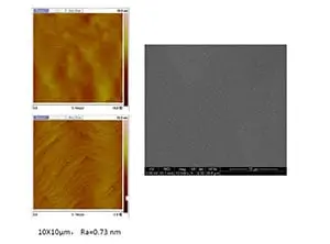
- Surface roughness below 1nm
- Single-side polished surfaces
- High crystal quality epitaxial films
Low roughness AlN films are especially important for epitaxial growth, thin film deposition, photonic structures, and semiconductor device fabrication.
AlN Templates for 2D Materials Research
Aluminum Nitride templates are increasingly used for the growth and characterization of 2D transition metal dichalcogenides (TMDCs), graphene, and advanced epitaxial semiconductor materials.
Highly insulating AlN templates allow researchers to study electrical properties and epitaxial growth behavior while minimizing unwanted substrate conductivity effects.
Typical research specifications include:
- Single crystal epitaxial AlN layers
- High resistivity substrates
- Single-side polished surfaces
- Custom polarity options
- Low surface roughness
- Sapphire or silicon substrate options
These AlN templates are commonly used in semiconductor research labs, university cleanrooms, and advanced photonics studies.
Surface Roughness and XRD Characterization
Surface roughness and X-ray diffraction (XRD) linewidth measurements are critical for evaluating AlN template quality. Low defect densities and smooth epitaxial surfaces are essential for UV LEDs, photonics, HEMT structures, and semiconductor wafer processing.
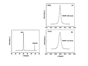
UniversityWafer can provide custom AlN surface roughness specifications, epitaxial layer structures, wafer diameters, and film thicknesses to support advanced semiconductor and materials science applications.
What is Aluminum Nitride?
Aluminum Nitride (AlN) is a ceramic semiconductor material with high thermal conductivity, strong electrical insulation, and a wide bandgap of approximately 6 eV. These properties make it valuable for microelectronics, RF devices, UV optoelectronics, and high-temperature semiconductor applications.

Aluminum Nitride is commonly used in:
- RF filters for mobile devices
- Piezoelectric resonators
- Acoustic wave devices
- UV LEDs and optoelectronics
- Infrared detectors
- Laser systems
- High-temperature electronics
- Power semiconductor devices
Because AlN combines high thermal conductivity with electrical insulation, it is considered one of the most important materials for advanced semiconductor and microelectronic technologies.