
I am looking for silicon 6” in size Have a NOTCH instead a  regular wafer flat (see details below) Clean for CMOS fab cleaning room operations. Si substrate preferred but don’t have to. Other layers on wafers probably don’t matter so long as they are compatible to CMOS fab. The quantity is likely 10 wafers or more. To be specific, the notch size that I am looking for is as the following. I guess its dimension is very likely a standard but need your expertise to judge. The reason I am buying Si wafers with notch is because I plan to use them as alternative wafers of SiC wafers in flat cut process development. Due to the expensiveness of SiC wafers, I use these test wafers as cheap alternative ones for initial wafer cutting test.
Silicon Wafer for CMOS Research
A scientist was in need of silicon wafers:
UniversityWafer, Inc Quoted:
Silicon Wafer
6", 650um, SSP, P<100>, 1-100 ohm-cm
Quantity: 10 Wafers
FOB Price: $Contact us for pricing
Get Your Quote FAST! Or, Buy Online and Start Researching Today!
Sapphire Wafers for CMOS Research
A materials scientist requested help with their questions:
There is some interest in the 150mm Sapphire Subsstrate r which you quoted last month. Are you able to specify / measure/ guarantee surface or bulk metals on sapphire wafers to a specification of <3E10 atoms/cm2 for the following heavy metals: Al, Cr, Cu, Ca, Fe, K, Ni, Na, Zn.
Do you have a cleaning process in place for heavy metal element control on the wafer surface?
Our customer would like to use the wafer in a CMOS compatible environment which requires contamination control of heavy metals. Do you have any more information regarding impurities in the bulk beyond the 99.996% purity specification?
Answer:
1. Are you able to specify I measure/ guarantee surface or bulk metals on sapphire wafers to a specification of <3E 10atoms/cm2 for the following heavy metals: Al, Cr, Cu, Ca, Fe, K, Ni, Na, Zn.
Rep: Actually,we do have the GDMS test report , like attached pic_‘GDMS test report“
But , regarding for the Metallic Contamination ,we do not have the tesgt date .
1stly ,we have contact the tester to check the 6 inch size of wafers by send the samples to American , will test by ICP-MS or VPD and the reference result will be get feedback several weeks manybe longer . We will feedback you the more details as soon as we get the test result .
2ndly ,maybe we also could send samples to your side to test/ check and could compare the test dates .
2. Do you have a cleaning process in place for heavy metal element control on the wafer surface?
Rep: Yes ,we do have the cleaning process to control the heavy metal element ,such as we use the H2SO4 / H2O2/semi-conduct purity wafer to cleaning the wafers ,We also control the heavy metal element by control the medicine /water .
Unlike Silicon, sapphire itself is less prone to metal ion adsorption.
3. Our customer would like to use the wafer in a CMOS compatible environment which requires contamination control of heavy metals. Do you have any more information regarding impurities in thebulk beyond the 99. 996% purity specification?
Rep: we have a GDMS / MSDS /ROHS test report for your reference ...Hope will be useful .. if you have any further question ,please feedback to me.
How do high-frequency CMOS chips manage heat dissipation from switching power loss?
High-frequency CMOS chips inevitably generate heat due to their dynamic (switching) power losses, which scale with frequency. Managing that heat is critical for reliable performance. Below is an overview of the most common techniques and design strategies used to handle switching power dissipation and the resulting thermal challenges:
1. Reducing Power at the Device and Circuit Level
a. Lower Supply Voltage
- Dynamic power is proportional to V2V^2. Dropping the supply voltage (VDD) is one of the most direct ways to curb switching power.
- This approach is central to modern process nodes, where nominal VDD has steadily decreased (e.g., from 5 V in older CMOS to below 1 V in advanced FinFET/FD-SOI nodes).
b. Minimizing Load Capacitance
- Dynamic power is also proportional to the load capacitance CC.
- Designers minimize parasitic capacitances through careful layout, using smaller transistors, shorter interconnects, and advanced device structures (e.g., FinFETs, GAA-FETs).
- Techniques like layout optimization and gate sizing further ensure minimal switching capacitance.
c. Reducing Switching Activity
- Power also scales with the switching activity factor α\alpha. Not all gates switch on every clock cycle.
- Clock gating and power gating selectively shut off clock signals or entire circuit blocks when they are idle, significantly reducing dynamic power.
- Data gating or operand isolation can similarly reduce unnecessary toggling of internal signals.
2. Architectural and System-Level Techniques
a. Parallelism and Multi-Core Architectures
- Instead of pushing one core to extremely high clock frequencies, modern designs use multi-core architectures running at moderate frequencies.
- This approach spreads out workload (and heat generation) while avoiding the exponential increase in power associated with very high frequencies in a single core.
b. Dynamic Voltage and Frequency Scaling (DVFS)
- Systems monitor workload and temperature to dynamically adjust clock frequencies and supply voltages on the fly.
- When high performance is needed, voltage and frequency go up; during idle or light load, they go down—managing both power and heat.
c. Thermal-Aware Floorplanning
- During the physical design (place-and-route) stage, high-power blocks are distributed to reduce localized hotspots and improve overall heat spreading.
- Critical analog, memory, or other blocks might be placed strategically for better thermal management (e.g., near heat sinks or away from other hot blocks).
3. Packaging and Cooling Solutions
a. Advanced Packaging
- Flip-chip ball grid array (FC-BGA) packages place the silicon die face-down onto the package substrate, which shortens interconnect lengths and provides better thermal conduction paths.
- 3D stacking (through-silicon vias, TSVs) includes careful thermal considerations because stacking can concentrate heat in small volumes.
b. Heat Spreaders, Heat Sinks, and TIM
- Integrated heat spreaders (IHS) on top of the die help conduct heat to larger external surfaces.
- Thermal interface materials (TIMs) (greases, gels, phase-change materials) improve conduction from the chip to external heat sinks or cold plates.
c. Active Cooling Systems
- High-performance systems often rely on fans, vapor chambers, or liquid cooling to extract heat from the CPU/GPU package.
- Data centers may use immersion cooling or specialized chilled-water cooling loops for extremely dense compute solutions.
4. Advanced Transistor and Process Technologies
a. FinFETs and GAA (Gate-All-Around)
- These 3D transistor structures improve electrostatic control, lowering both leakage current and some parasitics, which in turn reduces the overall power.
- Better subthreshold swing helps keep supply voltages lower while maintaining performance, thus reducing both dynamic and static power.
b. FD-SOI (Fully Depleted Silicon-On-Insulator)
- The thin oxide layer in SOI processes reduces parasitic junction capacitances, lowering dynamic switching losses.
- Designers can also apply back-bias to adjust transistor thresholds dynamically, balancing performance and power.
5. On-Chip Power Distribution and Regulation
- On-die voltage regulators (e.g., low-dropout regulators or switching regulators) can provide fine-grained voltage domains.
- Smaller, localized power domains help regulate supply precisely, minimizing both IR drops and unnecessary power consumption.
6. Design Tools and Methodologies
a. Power Analysis and Profiling
- Electronic design automation (EDA) tools perform static and dynamic IR drop analysis and thermal simulations.
- Early in design, power analysis tools predict hotspots and guide design decisions (e.g., block placement, timing constraints).
b. Power-Aware Synthesis
- Synthesis tools optimize logic at the gate level with power-specific objectives, balancing timing closure and minimal switching power.
Putting It All Together
- Reduce the causes of switching power: Lower the supply voltage and minimize parasitic capacitances.
- Control switching activity: Employ clock/power gating and advanced architectural techniques (e.g., multi-core, DVFS).
- Enhance heat extraction: Use advanced packaging, heat spreaders, and, if necessary, active cooling solutions.
- Optimize transistor technology: Transition to FinFETs, GAA-FETs, or FD-SOI to reduce both dynamic and leakage components.
- Design for thermal awareness: Floorplanning and EDA-driven optimization ensure that local hotspots are minimized.
These strategies collectively allow modern high-frequency CMOS chips to manage heat dissipation from switching power losses, enabling the ever-increasing performance demands of today’s semiconductor industry.
Is It Difficult to Beat Silicon for Complementary Metal Oxide Semiconductors?
CMOS (Complementary Metal Oxide Semiconductor) is a technology that uses two different combinations of metals in the construction of integrated circuits. It is used in transistors in computer microchips, and is increasingly important in applications such as automotive and image sensors. It is expected that the use of CMOS will increase significantly with the increasing popularity of smartphones. Regardless of its benefits, it remains difficult to beat silicon when it comes to performance.
A typical complementary metal oxide semiconductor (CMOS) has an electronic rolling shutter design. In this 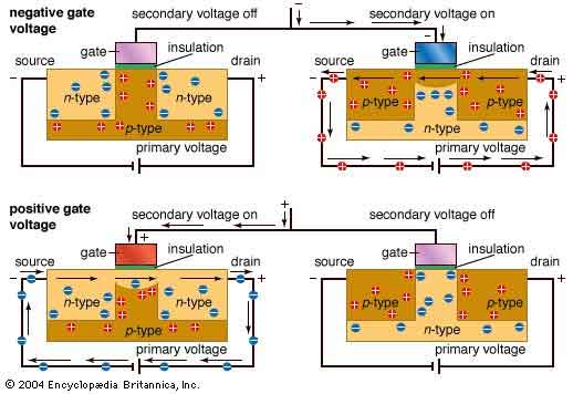 design, data is not passed from one bucket to another, but rather is read from one bucket to the next. The CMOS sensor implements an electronic rolling slit shutter by causing a reset on each row. This process limits the speed at which the wave passes over the sensor. In order to make all rows of CMOS devices equally exposed, the waves must precede each other.
Despite the success of CMOS, the technology is facing fundamental scaling limitations. While Moore's law pushed down the cost of integrated circuits, it also caused a rise in power consumption. To overcome this scaling problem, new strategies are needed. These include the "More than Moore" and "Beyond CMOS" strategies. The resulting product is more efficient and has lower power consumption than the competition.
CMOS-MOS technology combines a p-type and n-type metal oxide semiconductor to produce an integrated circuit. This design technology is commonly used for RF and digital logic circuits. It is also used for image sensors, data converters, and highly integrated transceivers. The advantages of this semiconductor technology are numerous and many. However, the downside is that it is difficult to scale, making it a challenging and expensive option.
A complementary metal oxide semiconductor (CMOS) is a semiconductor that has complementary symmetry. It is a type of MOSFET that uses a complementary pair of p-type and n-n-n junctions to form the transistor. It is widely used in digital logic circuits, and is an ideal choice for mobile devices and cameras. Its high-performance capabilities make it an ideal material for a variety of applications.
CMOS technology has been the standard for decades. Unfortunately, it is nearing its limits, and other semiconductors will need to find innovative solutions to this challenge. In addition to the intrinsic strengths of silicon, CMOS-based semiconductors are also cheaper and more efficient. The current generation of CMOS chips is expected to surpass the performance of the III-V semiconductors in the next few decades. They can be fabricated in larger quantities, and can be etched into smaller areas.
Complimentary metal oxide semiconductor (CMOS) technology is the basic logic controller of integrated circuits. Its high integration and low power consumption makes it the preferred material for a wide variety of applications. The CMOS technology is also a great choice for a number of other applications, such as image sensors and CMOS image sensors. The CMOS technologies are becoming the standard in smartphones, but they are still limited by their power limitations.
CMOS-based silicon technology is facing fundamental scaling limitations. While the Moore's law has enabled high integration and performance without reducing power consumption, this trend has led to a steep decline in the power of the devices. As a result, new strategies are needed for the semiconductor industry to continue to grow. Several emerging CMOS technologies are being developed to address these challenges. The first generation of CMOS uses copper, while a complementary metal oxide semiconductor uses an iron-based alloy.
In terms of power consumption, the complementary metal oxide semiconductor (CMOS) is a type of semiconductor with low power consumption. This technology is used for analog and digital ICs and is gaining popularity with smartphones and mobile devices. Because of its low power consumption, it is also used in other applications, including wireless communications and memory. The technology is gaining more popularity in consumer electronics. These devices are becoming increasingly useful and popular as everyday products.
What is CMOS?
What is Cmos? It is a semiconductor device, which is made from a combination of two materials. The p-type MOSFETs are connected by a metal gate and are used in computer circuits. A CMOS chip is a small electronic device which can be produced using multiple manufacturing techniques. The CMOS process is also known as complementary-symmetry metal–oxide-semiconductor.
In a CMOS system, a number of different components are linked to each other by logical gates. These 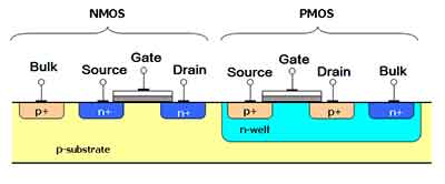 electrical components are called 'bits'. The CMOS style is used in constructing computers and is governed by a set of rules that writers should follow. When writing about CMOS, the word 'CMOS' refers to a chip that is made of a combination of several transistors.
The CMOS process is used in a large number of computer systems. It is used to develop written standards for communication between components. CMOS is used in the manufacture of most current processors. CMOS memory in a computer is a type of nonvolatile RAM that stores time and BIOS settings. It also has many uses and is an excellent choice for storing a large number of files. If you are thinking of buying a new computer, remember that the CMOS process is very important.
The CMOS format for writing has rules that students and writers should follow. In general, CMOS equipments have two independent environments and a Drop-down network. The logical gates are united in a circuit to form the device. The PLIN and PDN transistors are similar to each other, but each has its own advantages. The NB and AD systems use notes and NB and AD systems are almost identical.
CMOS is vital for the proper operation of a computer, but you should not make any changes without understanding how they impact the CMOS. You should take a backup of your BIOS settings and make a copy of it before you begin. You should never change the CMOS setting unless you are sure you know exactly what you're doing. This way, you can easily recover from any error that has occurred due to a CMOS reset.
CMOS is an integral part of the computer. It is the main memory of the computer. It stores the BIOS settings and hardware settings. A CMOS battery requires a special section of the motherboard for the CMOS battery. This section is usually accessed by a small wire. The CMOS battery is stored in a separate section and connects to the motherboard with a wire. There are two ways to remove the CMOS. One is to disable the chip.
CMOS is the key to the functioning of a computer. The CMOS chip contains the ROM and the RAM. The ROM is the ROM. Unlike a BIOS chip, CMOS doesn't have a memory. In fact, a CMOS chip is not a real BIOS. It is an entirely different system. It's used by a number of devices to control the computer and make it run.
CMOS is a semiconductor that works with two different types of transistors. The N-Channel MOSFET conducts when the P-Channel MOSFET is off. Both types of CMOS transistors are monolithic, and require a power source. A CMOS chip's CMOS RAM requires its own power supply. Although CMOS is considered a low-power device, it uses a small amount of electricity to operate.
CMOS is the small battery-powered integrated circuit on a computer's motherboard. The CMOS chip stores the hardware system settings and BIOS settings. It's also a key component of a modern PC. CMOS is an important component of powerful computer chips. But the CMOS chip's memory is not only crucial for a computer's operation. Even a simple CMOS battery can help save the day and a computer.
A CMOS chip is a semiconductor that stores basic information in a computer. It stores the date and time, as well as the system's configuration. Its CMOS chip can be used in many different applications, from auto stamping to wireless communications. The DECT cordless phone has RF CMOS chips from Intel. There are thirty-four companies that manufacture CMOS chips. When you use a cellular phone, you can connect it to the RF amplification chip.
What is a CMOS Used For?
When you are looking for a good computer parts store, you can find a wide variety of CMOS devices. A  CMOS chip is a semiconductor chip that contains a number of different circuits. Its main function is to set up the computer, load the drivers, and boot the operating system. CMOS is also used to configure BIOS settings, which is why it is crucial to understand how these devices work.
CMOS stands for complementary metal oxide, which is used to create a circuit that can perform various functions. In a computer, a CMOS battery is used to store the basic information of a computer. The information it stores is vital for the functioning of the computer. It stores the time, hardware, and BIOS settings. It is also used to control the amount of power that a computer uses.
A CMOS chip is used to control the amount of memory on a motherboard. A CMOS chip can be used to set the time, date, and hardware settings. It also has a high noise margin. CMOS chips are used to control the amount of memory available on a motherboard. A CMOS is used to store settings, including the date, time, and hardware. The CMOS has become one of the most important parts of a computer.
CMOS technology is gaining ground in the electronics industry. The CMOS chip is a small piece of memory on a motherboard that stores information, such as the BIOS settings and the time. Some of the CMOS chips are made by over thirty companies. If you're wondering, "What is a CMOS?" just take a look at the many examples. They're useful for so much more than just computer parts!
CMOS power supply pins are used for dissipating power. They are referred to as VSS (voltage-switching) and VDD (source-supply voltage). They are used in circuits that use capacitance. The CMOS IC is also used in computers. The CMOS is a good choice for a lot of electronic components. They're widely used in many types of industries, from smartphones to medical devices to automobiles.
CMOS is short for complementary metal oxide semiconductor. It stores BIOS settings and cellular system settings. A CMOS is also used to store information on a computer. You can get a CMOS chip for your computer from most electronics vendors. The CMOS chip is an important part of a cellular system. However, if your CFOS is not working correctly, it can affect your computer.
CMOS chips use a complementary metal-oxide-semiconductor (CMOS). This type of CMOS is used for many technical applications. It is a great way to convert light waves into digital signals. CBCT takes images in slices and then combines these slices to create a 3D reconstruction of a patient's anatomy. If you're using a CBCT device to scan a patient, a CMOS chip is an excellent option.
CMOS is a semiconductor chip that is used for many purposes. Its main function is to store system settings and BIOS settings. Other CMOS chips are used in camera sensors. They are battery powered and can be found in laptops and computers. Similarly, CMOS is the most common type of semiconductor chip in a CMOS. There are several other uses for CMOS in a computer.
CMOS chips are commonly used in the semiconductor industry for a variety of applications. They are used for a variety of purposes, including digital logic ICs and analog mix and signal ICs. A CMOS chip uses a CMOS technology that can operate at very low costs. The CMOS process is very efficient and helps computers run at full speed. With CMOS, a CMOS chip is much faster than a transistor.
CMOS is a semiconductor chip that is used to store important information for a computer. It is the key component in a microprocessor, and stores all of the necessary information for the system. CMOS chips are commonly used in microcontrollers, image sensors, and high-integrated transceivers. If you are looking for a CMOS, you have come to the right place.
How Does a CMOS Image Sensor Work?
CMOS image sensors use multiple transistors to create an image. Each pixel in the image has its own charge. The amount of light falling on the pixel produces a different amount of charge, which is then read by the analog-to-digital converter. The resolution of a CMOS image sensor is determined by the number of pixels and their intensity. The next step is to read the individual value of a pixel, which is called integration.
CMOS image sensors work by converting light into electrical signals. The photodiode array generates  photoelectric signals, which are then sent to the analog-to-digital conversion circuits, located adjacent to the photosensitive region. In addition to generating voltage, a CMOS image sensor also has many other duties. It is used in video cameras to store digital images. However, it must be understood that a CMOS image-sensor pixel has a lot more complexities than it appears at first glance.
The CMOS active sensor pixel consists of a three-dimensional cutaway diagram, which shows the photosensitive region, busses, and the Bayer filter. It has three transistors for each pixel, and each of these has its own set of features. Each of these elements contains an amplifier transistor and represents the input device to a source follower. The source follower converts the electrons produced by the photodiode into an electrical signal. This voltage is output to a column bus.
CMOS image sensors work on a standard silicon process. During this manufacturing process, the chips are placed onto a silicon wafer foundation. Often, a CMOS chip is fabricated with the same silicon foundation as digital logic circuits and analog-to-digital converters. In addition, CMOS image sensors participate in shrinking processes. To reduce cost and increase performance, the CMOS manufacturing process is modified.
CMOS image sensors work by generating and measuring the voltage and the light intensity. In order to measure the brightness and color of an object, a CMOS image sensor detects both the horizontal and vertical movement of the camera's image. This data is converted into an analog signal and transmitted to the display. A CMOS camera's color sensitivity is based on the intensity of light it captures.
The CMOS image sensor works by detecting the light passing through it. Its pixel electrical signal is amplified before sending it to a correlated double-sampling (CDS) circuit. The photo-sensitive region of a CMOS image sensor is composed of multiple MOS tubes. These tubes form a single pixel, which is called a pixel. A CMOS image sensor includes a horizontal and vertical shift register.
A CMOS image sensor is a semiconductor device that converts light to an electrical signal. The CMOS image sensor is also similar to a CCD, but it has different components. Unlike a CCD, a CROS image sensor uses a PN junction instead of a pixel. In contrast to a CCD, a CMOS image sensor can process multiple color signals and transmit them faster than a traditional pixel.
CMOS image sensors are a combination of multiple pixel arrays and a CMOS image sensor has two different outputs. Each pixel has an amplifier transistor. Each pixel receives a voltage from the light. A CMOS pixel is a CMOS photosensor. A CMOS photosensor is a very useful tool for photography and filmmaking. This technology is also used in digital cameras.
A CMOS image sensor uses an array of microlenses to capture light. The photodiodes in a CMOS image sensor are organized into an orthogonal grid. The pixels on a CMOS chip are typically arranged one-by-one. The size of the pixel determines the sensitivity of the device. Besides capturing light, CMOS image sensors also reduce static electricity discharges.
CMOS image sensors have a range of different functions. For example, CCD image sensors are able to capture a wide range of wavelengths and use a multi-spectral image to capture light. A CMOS image sensor can be useful for a wide variety of purposes. It is also useful for video recording. Its high dynamic range makes it a great choice for digital cameras.
What Substrates Are Used to Fabricate CMOS Sensors?
What substrates are used to fabricate CMOS sensors? These semiconductor devices are  manufactured on silicon wafers. These semiconductor wafers are also known as CMOS monolithic pixel sensors. There are two types of CMOS substrates. The first one is called an epitaxial wafer and the other one is referred to as a non-epitaxial high resistivity type.
These CMOS sensors are made by stacking a large-area silicon die and a deep n-well. The electronics are disposed inside the n-well. A high-resistivity p-substrate is used in this type of CMOS device. This CMOS sensor is a good choice for applications that need high radiation tolerance and low noise.
CMOS monolithic active pixel sensors are designed to withstand high radiation environments. They are built with a radiation-sensitive detector element and front-end readout electronics. The prototype DMAPS was fabricated in a 150nm CMOS process with a thinning process to 100 mm. The DMAPS was fabricated using a direct deposition process. The epitaxial substrate is used for prototypes. The epitaxial substrate is composed of a thin layer of p-doped silicon that is bonded to the top surface of the chip. The TSV technique was employed at Lincoln Laboratories.
CMOS monolithic active pixel sensors are charged particle tracking devices that integrate the radiation-sensitive detector element with the front-end readout electronics. These CMOS devices are fabricated using submicron and deep submicron commercial CMOS processes. They are directly ready for use without the need for post-processing. To fabricate these sensors, a thin epitaxial substrate is used. A p-doped silicon layer is used as the base substrate.
CMOS image sensors use a p-substrate and a deep n-well. This technology makes the n-onp sensor a layered structure. The two types of CMOS photosensors are typically built from a p-substrate with a n-well. When fabricated on an epitaxial substrate, the semiconductors are completely flat.
CMOS Monolithic active pixel sensors are a type of CMOS sensor that integrates a charge-sensitive detector element with front-end readout electronics. The CMOS image sensor is designed using standard microelectronics CAD software. It is fabricated with a commercial submicron CMOS process. It is direct-use ready with no post-processing.
The CMOS sensor uses a p-substrate with a deep n-well. The p-substrates have high resistivity and are commonly used to fabricate CMOS n-on-nap sensor technology. They are both made of silicon, and can be fabricated into high-precision n-on-p n-nanosensors.
The CMOS sensor's surface is superhydrophobic, so that the EV solution can only contact a small area of the sensor. The EVs are only dry on a small area of the substrate, so that the n-nanostructured CMOS sensor can be fabricated easily and inexpensively. In addition, the p-nanostructured CMOS structure is very similar to an epitaxial p-nap-nap-nap n-nap-p-nap-nap sensor.
CMOS sensors are fabricated on a p-n-p substrate. The n-on-p substrate is made of a p-substrate with a deep n-well. The electronics are placed in the deep n-well, while the p-n-p type is made of silicon. This n-on-p CMOS technology has the advantage of using a wide variety of amorphous silicon epitaxial substrates.
Another CMOS sensor is the depleted monolithic active pixel sensor. It is a CMOS sensor with both the sensing diode and readout electronics in the same CMOS wafer. This technique is based on a depleted region with a sufficient thickness. The size of the depleted region depends on the size and the reverse bias voltage applied.
CMOS sensors are fabricated on a variety of substrates. The p-substrate is a very important component of a CMOS sensor. This type of sensor can be manufactured on silicon, alumina, or glass. A typical CMOS sensor has a p-substrate resistivity of 100 nm. A CMOS-based NMOS sensor is made on a p-substrate of 78 nm with a thickness of 280 nm.
What Is CMOS and What Are the Benefits of CMOS?
What is CMOS? It is a battery-powered integrated circuit that stores BIOS and Clock/Date settings and maintains a real-time clock. What are the benefits of CMOS? Learn how CMOS can improve your computer's performance. Here are three major benefits of CMOS:
CMOS is a battery-powered integrated circuit
CMOS is a battery-powered, integrated circuit that stores basic computer information. It controls the Power On Self Test and runs a series of tests when the computer starts. One of these checks counts up the amount of random-access memory in the computer. Counting RAM slows down boot time. To speed up boot time, disable counting RAM when installing new RAM. Otherwise, your computer may not boot up properly.
CMOS was first developed in 1968 by Fairchild Semiconductor, and RCA released its first CMOS-based integrated circuits in 1968. At the time, CMOS was developed as a low-power alternative to TTL technology, and the battery-sensitive watch industry embraced CMOS's potential as a lower-power alternative. CMOS has since gone on to become the dominant technology for digital integrated circuits. In addition, it has been geometrically downsized with each new semiconductor manufacturing process.
CMOS stands for metal oxide semiconductor. CMOS circuits combine n-channel and p-channel devices. Compared to the TTL and ECL logic series, CMOS circuits have a better average propagation delay. This is especially useful in battery-powered integrated circuits. CMOS is more efficient than TTL and ECL, and it can be used with a five-volt supply. The cost of CMOS equipment is relatively high compared to other technology options.
CMOS is an important type of integrated circuit, which is used to create real-time clocks, non-volatile RAM, and BIOS memory in your computer. This technology has a long life span, and is capable of lasting as long as the battery power supply does. The only drawback of CMOS is that it does not save time after the computer is turned off. This makes it a valuable part of your computer's hardware.
CMOS devices are low power, primarily because their power consumption is minimal. The parasitic capacitor embedded in CMOS gates is responsible for the bulk of the power consumption. CMOS devices have very low static power consumption and a low leakage current when the circuit is not charging or discharging. Dynamic power consumption is increased when the output load is charging or discharging, so it is important to consider this when designing the circuit.
When a CMOS malfunctions, the system will not be able to understand which boot device is the priority. A computer will display errors as it attempts to boot. In addition, it may cause your customized keyboard configuration to be reset. CMOS failure can also prevent your internet connection. BIOS manages network and hardware drivers. If it fails, these devices will not work. If your CMOS battery is low, it is essential to replace it as soon as possible.
CMOS devices are designed to minimize power consumption. Low power consumption makes the device more reliable. To minimize power consumption, you should learn how to calculate the voltage level, rise time, and output loading. These factors will determine the total power consumed by the CMOS device. You can also look for ways to reduce this power consumption and keep it as low as possible. There are many factors that can affect power consumption.
It stores BIOS and Clock/Date settings
If you need to reset your PC's BIOS settings, you can clear the CMOS, the computer's memory that stores these important settings. This is a quick and easy troubleshooting step, and can help you fix many problems, including freezing during the POST process, hardware-related error messages, and CMOS checksum. However, if you don't have the CMOS battery, this method may not work for you.
CMOS, or complementary metal oxide semiconductor, is the chip responsible for storing BIOS and clock/date settings on the computer. The CMOS chip contains a small amount of information, typically 256 bytes, and controls your computer's hardware. The data in the CMOS chip includes your boot priority, your computer's system configuration, the time and date, and your BIOS administrative password. Some motherboards have a separate CMOS chip, while others combine the function with the RTC.
CMOS is a small piece of static memory that resides on a chip alongside the Real-Time-Clock. The IBM PC AT, for example, didn't have a CMOS chip. Instead, its BIOS settings were controlled by DIP switches on the motherboard. The IBM PC AT used a Motorola MC146818A real-time clock, a 64-byte memory that included both a clock and alarm time.
It maintains a real-time clock
A CMOS chip contains a small amount of memory which is programmed to access a CMOS value, one byte at a time. These values are referred to as "registers" and the first 14 of these are used to access the Real-Time Clock. The only CMOS register which is really useful is register 0x10. All other CMOS registers are almost obsolete and not standardized.
A computer motherboard contains a microchip which houses the real-time clock. This chip is separate from the microprocessor and stores a system description and current time values. The real-time clock includes information about the day of the week, month, and year. It also stores the Basic Input-Output Operating System (BIOS) and BIOS (BIOS).
While real-time clocks are used in computers, they are also found in many simpler electronic devices. This functionality of real-time clocks is essential for the functioning of computers and other electronics. Time measurement is used in almost every aspect of computing. Traditional clocks and watches use an RTC module to keep track of the time. A real-time clock module can also be found in most computers. The RTC module is an essential part of a computer.
Video: What is CMOS and What Is It Used For?
What Substrates are Used for CMOS Voltage Converter?
Scientist have purchased the following wafer spec for their research.
Single-side-polished (100) silicon wafers (University Wafer, South Boston, MA) were used as deposition substrates for ellipsometry, atomic force microscopy (AFM), and scanning electron microscopy (SEM). Silicon wafers were piranha treated with 3:7 30% hydrogen peroxide to 99% sulfuric acid ratio and stored in deionized water before being used. Caution: Piranha solution reacts violently with organic material and needs to be handled properly. Prior to use, the silicon wafers were rinsed with acetone and deionized water. Poly(ethylene terephthalate) (PET) film with a thickness of 179 μm (trade name ST505, Dupont–Teijin) was purchased from Tekra (New Berlin, WI). A 175 μm polystyrene (PS) film (Goodfellow, Oakdale, PA) was used as a substrate for transmission electron microscopy (TEM). Both PET and PS films were rinsed with deionized water and methanol before use. Cleaned PET and PS substrates were then corona-treated with a BD-20C Corona Treater (Electro-Technic Products Inc., Chicago, IL). Corona treatment improves adhesion of the first polyelectrolyte layer by oxidizing the film surface.197 Polished Ti/Au crystals with a resonance frequency of 5 MHz were purchased from Maxtek, Inc (Cypress, CA) and used as deposition substrates for quartz crystal microbalance (QCM) characterization.
Pelase contact us for specs and pricing.
What is a CMOS Voltage Converter?
CMOS Voltage Converters can provide both positive and negative supply voltages. A negative  supply voltage is desired when a system has ground-referenced signals and digital logic. While this requirement is relatively low, a negative supply voltage can be extremely expensive and inefficient. This circuit converts the positive and negative supply voltages using only two non-critical capacitors. If the input voltage is higher than 6.5V, a diode is added to protect the device.
What is the Meaning of CMOS?
CMOS is an acronym for complementary metal oxide semiconductors. These semiconductors are used to convert light into electrical signals, similar to charged image sensors. They are used in computer memory chips, battery-powered cell phones, and even in BIOS settings. As their name suggests, they have a low gate-source threshold voltage. CMOS memory chips are made using metal oxide semiconductors. To learn more about CMOS, read on!

CMOS is a battery-powered memory chip
CMOS is a battery-powered storage device that stores the computer's memory. Depending on the model, a CMOS battery will last for two to 10 years. However, if the battery dies, the CMOS chip will automatically be reset, losing any custom settings. In addition, CMOS battery-powered computers will lose the BIOS settings when not plugged in. A CMOS chip typically stores 256 bytes of data and is powered by a coin-sized CR2032 cell battery.
A CMOS memory chip is used to store basic system information, including the configuration of the hard drive and the time and date. In addition, it provides a real-time clock and memory. These are some of the most important functions of a computer. But they do a lot more. Here's how CMOS memory works:
A CMOS battery keeps track of the motherboard's configuration data, and is also responsible for the computer's Real Time Clock. A battery also helps power the CMOS chip, which is a crucial part of a computer's operating system. If the battery dies, the computer will not be able to boot from its hard disk. Fortunately, battery-powered CMOS chips have backup batteries, which means that if your computer does lose power, you can simply replace the battery and still continue to use the device.
A CMOS is a type of semiconductor that uses complementary metal oxides (MOS) and polysilicon layers to store information. CMOS chips are used in various integrated circuits, including those used in mobile phones. When a CMOS chip fails, it loses the clock and the BIOS settings. It is important to know about these types of chips before replacing your CMOS.
If your CMOS battery fails, you need to restart your computer to clear the settings in BIOS. You can do this in the BIOS menu, but you may need to remove the case to access the CMOS chip. The CMOS chip also stores system clock and disk drive information. Some motherboards have the CMOS chip separately, while others include it with the RTC on the south bridge.
CMOS uses metal oxide semiconductor field-effect transistors
Complementary metal-oxide-semiconductor (CMOS) technology uses two different types of transistors, a type called a MOS. These devices operate by utilizing opposite-polarity electrons, and thus are able to lower power consumption and allow for efficient, low-power memory storage. The process began in 1960, with Mohamed Atalla and Dawon Kahng demonstrating a working device. Several years later, the NMOS process was developed and was much faster than CMOS, and was soon displaced by CMOS technology.
CMOS technology uses a patented process that allows manufacturers to manufacture devices with a wide variety of features and capacities. These devices have many different benefits. Unlike conventional semiconductors, they are made of a material that does not suffer from any type of electrical noise or interference. Their low-power characteristics make them an excellent choice for many types of applications. CMOS is an important advancement in semiconductor technology and has made a significant impact on the development of microelectronic devices.
The two types of CMOS technology differ slightly in their operation. The former uses a metal-oxide semiconductor channel with a silicon gate. The latter is a double-diffused metal oxide semiconductor. It is a type of semiconductor with a bandgap the same as the silicon channel. Because of this, it is capable of modulating its work function, allowing it to control low threshold voltages without affecting the functioning of preceding circuits.
A MOS device has a layered structure, and its gate is made of a metal or polysilicon material. Its electrical conductivity is controlled by the voltage applied at the gate terminal. Its ability to change its conductivity can be used for amplifying electronic signals. There are several other benefits of a MOSFET, and they are worth learning more about this technology. The next article will discuss its advantages.
One of the most important advantages of MOS is its miniaturization. A CMOS chip with 45 nm technology can have twice as many MOSFETs as a chip with 65 nm technology. This phenomenon, known as Moore's law, allows transistors to be smaller while still performing the same function. Its shrinking size has other advantages, including faster switching. In order to create smaller transistors, the main dimension of a MOSFET must be decreased proportionally. The major device dimensions are the channel length, the width of the oxide layer, and the thickness of the oxide layer. The smallest transistors will not only reduce the transistor's overall size, but also decrease the device's gate capacitance.
CMOS reduces power consumption
CMOS is a type of integrated circuit that greatly reduces power consumption. Its power consumption is directly proportional to its clock frequency, which can be controlled dynamically to decrease power usage. Such control can be implemented at the hardware level, or can be managed by the operating system. Some hardware devices and systems have sleep or idle modes, in which they are not in use. Wake-up events are used to wake up the device from sleep or idle mode. Depending on the device, the wake-up time may vary as well.
The difference between pMOS and nMOS is in the rise and fall time of the transistor. During the rise time, the pMOS transistor conducts, while the nMOS transistor conducts only at the maximum frequency. As the pMOS transistor conducts in a weaker region, it inhibits current flow between VDD and GND. When the rise and fall time window is extremely small, or in nanoseconds, the short circuit power dissipation can be ignored.
Today's microchips have more than ever, and computing power is increasing at a faster rate. As a result, power consumption is a major concern for CMOS circuit design. It is critical to find methods to reduce power consumption while still delivering the desired performance. Listed below are some techniques for designing with low-power CMOS circuits
Variable-threshold CMOS circuits also minimize static power dissipation and leakage. They are easier to implement than discrete devices, and their basic principle is to keep the substrate from the source and apply a different voltage to it. Besides, the CMOS chip has a much higher density of logic gates than the TTL chip. Despite its low-power consumption, CMOS is susceptible to static electricity.
CMOS has a low gate-source threshold voltage
The gate-source threshold voltage in CMOS is typically low. The threshold voltage is affected by the doping concentration and temperature. In fact, a change of 30 degC in the ambient temperature results in a change of over 3 mV compared to the 500 mV design parameter for GaAs MOSFETs. Consequently, it is necessary to increase the gate-source threshold voltage in order to achieve the desired inversion.
A negative gate-source threshold voltage reduces the amount of charge on the semiconductor layer. This allows electrons to flow freely in the channel. This property is also known as the ease-of-flow threshold. It's very important to understand how to design digital circuits involving MOSFETs because a lower gate-source threshold voltage results in a lower drain-source current. This phenomenon makes it necessary to increase the threshold voltage in order to create efficient digital devices.
However, the currents of I2 and I3 dominate the off-leakage. The leakage current is a function of both Vgs and Vds. The highest leakage current occurs when Vgs is maximum and Vds is zero. Therefore, increasing the threshold voltage increases the speed of switching while reducing the leakage power. The trade-off between power consumption and performance is linear.
When determining the voltage of the device, the bulk terminal has the greatest effect on the channel potential. This effect is especially important in thick gate oxide. Bulk biasing is a common technique used to reduce the gate-source threshold voltage. It involves increasing the voltage across the bulk-source PN junction, reducing the gate-source voltage. It may require extra current to reach this voltage. However, lowering the gate-source threshold voltage by increasing the bulk-source voltage does not always lead to a low gate-source threshold voltage.
A high-quality semiconductor device requires a low gate-source threshold voltage to operate at its optimal level. A low gate-source threshold voltage is required for high-speed communication systems. High-speed communications require large gate leakage currents, which means that the gate-source threshold voltage is also low. By increasing the gate-source voltage, transistors can operate in either depletion or enhancement modes.
Video: What is CMOS?
What are CMOS Chip?
CMOS (Complementary Metal-Oxide-Semiconductor) chips are a type of integrated circuit that use a combination of metal, oxide, and semiconductor materials to build electronic circuits.
The key feature of CMOS technology is that it uses two types of transistors, known as n-type and p-type, to implement logic gates and other circuitry. This makes CMOS circuits very power-efficient, as they consume very little energy when not actively switching between states.
CMOS chips are used in a wide range of electronic devices, including microprocessors, memory chips, and sensors. They are particularly well-suited for battery-powered devices and other applications that require low power consumption. Additionally, their ability to integrate large numbers of transistors onto a single chip has made them a key component in modern electronics.
Substates Used to Fabricate Complementary Metal Oxide Semiconductor Memory
Complementary Metal Oxide Semiconductor (CMOS) memory is an integrated circuit (IC) technology widely used in digital electronics due to its low power consumption and high noise immunity. The most common substrates used for CMOS memory fabrication include:
Silicon: Silicon is the most widely used substrate material for CMOS memory fabrication due to its excellent electrical and thermal properties and abundant availability. Single-crystal silicon wafers with a specific crystal Ori, typically (100) or (111), are used as the starting material for CMOS memory fabrication. The silicon wafers are doped with specific impurities to create p-type or n-type regions, depending on the desired electrical properties of the final device.
Silicon on Insulator (SOI): A specialized type of substrate consists of a thin layer of silicon on top of an insulating layer, typically made of silicon dioxide. A bulk silicon or other substrate material then supports the insulating layer. In CMOS memory fabrication, SOI substrates reduce parasitic capacitance and leakage currents, resulting in improved device performance and reduced power consumption. SOI technology is advantageous for advanced CMOS memory devices with smaller feature sizes.
Germanium and III-V semiconductors: Although silicon is the most common substrate material for CMOS memory, alternative materials like germanium and III-V semiconductors (such as gallium arsenide, indium phosphide, or gallium nitride) are being explored for their potential to improve device performance. These materials offer higher electron mobility, leading to faster device operation and lower power consumption. However, challenges related to cost, material compatibility, and integration with existing CMOS processes have limited the widespread adoption of these alternative substrates for CMOS memory fabrication.
In summary, silicon is the most widely used substrate for fabricating CMOS memory devices, followed by SOI as a specialized substrate for high-performance applications. Alternative materials such as germanium and III-V semiconductors are also being researched for potential improvements in device performance.
What are some possible materials to replace CMOS after graphene and carbon nanotubes?
In the quest to replace CMOS (Complementary Metal-Oxide-Semiconductor) technology for building more efficient and powerful electronic devices, researchers have been investigating a wide variety of materials other than graphene and carbon nanotubes. Here are some materials and technologies that are considered potential successors to CMOS:
1. New Semiconductor Materials
-
2D Materials Other Than Graphene: This includes materials like molybdenum disulfide (MoS₂) and tungsten diselenide (WSe₂), which have shown potential in transistor applications.
-
Black Phosphorus: This material has been found to have excellent electronic properties and has been researched for its use in transistors.
-
Silicene: It is a two-dimensional allotrope of silicon and has properties similar to graphene.
-
Germanene: Similar to silicene, this is a two-dimensional allotrope of germanium.
2. Spintronics
-
Topological Insulators: These materials behave as insulators in their interior but support conducting states on their surface, offering new possibilities for transistor design.
-
Magnetic Materials: Materials that leverage electron spin rather than charge can be used in spintronic devices.
3. Quantum Materials
- High-Temperature Superconductors: These materials can conduct electricity without resistance at relatively high temperatures, promising energy-efficient technologies.
4. Emerging Computing Paradigms
-
Phase-Change Materials: These materials can change their physical properties based on external conditions, opening up avenues for novel memory and computing technologies.
-
Memristors: These are two-terminal non-volatile memory devices that store and process information similarly to the way synapses work in biological systems.
5. Quantum Computing
-
Superconducting Qubits: Materials such as Josephson junctions, which are made from superconductors, are used in quantum computers.
-
Topological Qubits: These rely on particles called anyons, which are theoretically predicted to be extremely useful for stable quantum computing.
6. Organic Semiconductors
- Organic Molecules: There has been research into using specially designed organic molecules to create semiconductors.
7. Nanomaterials
-
Quantum Dots: Nanoscale semiconductor particles that have quantum mechanical properties.
-
Nanowires: These have potential applications in nanoscale transistors.
8. Perovskite Materials
- Halide Perovskites: These materials are being researched for a variety of applications including photovoltaics and light-emitting diodes (LEDs), and could potentially find uses in semiconductor devices.
Conclusion
While all of these materials and technologies hold promise, it is worth noting that they are largely in the research and development stage, and significant breakthroughs will be needed to make them viable replacements for current CMOS technology. It will be a combination of material discovery, technological innovation, and industry adaptation that will dictate the next leap in computing technology.