Customer Question: Is Indium Phosphide a Cubic Crystal?
A chemical engineering researcher studying molecular beam epitaxy (MBE) of thin films for electronic, optical, and magnetic materials requested a quotation for Indium Phosphide (InP) wafers and asked two common questions regarding crystal orientation.
Research Questions
- What does the [111A] orientation represent?
- Is Indium Phosphide (InP) a cubic crystal?
UniversityWafer Response
- The [111A] surface is the indium-terminated face, while the [111B] surface is the phosphorus-terminated face. These two crystal faces exhibit different surface chemistry and are selected based on the intended epitaxial growth or device fabrication process.
- Yes. Indium phosphide crystallizes in the zinc blende cubic crystal structure, making it an excellent substrate for epitaxial growth, optoelectronic devices, high-speed electronics, and photonic applications.
Get Your Quote FAST! Or, Buy Online and Start Researching Today!
Reference: Customer Inquiry #268498
Available Indium Phosphide Wafer
The original Item K661 has been discontinued. We currently recommend the following equivalent specification:
| Item |
Specification |
| HQ20 |
2" Indium Phosphide (InP) Wafer
Orientation: (111B) ±0.5°
Thickness: 350 ±25 µm
Undoped
Carrier Concentration: <3 × 1016 cm-3
Bow: <30 µm
Warp: <30 µm
Single-Side Polished
Backside Matte Etched
EJ Flats
Surface Roughness: <15 Å
Nitrogen-Sealed Single Wafer Cassette
|
Additional InP wafer orientations, diameters, dopants, carrier concentrations, epi-ready surfaces, and custom specifications are available upon request.
What Are Cubic Crystal Substrates?
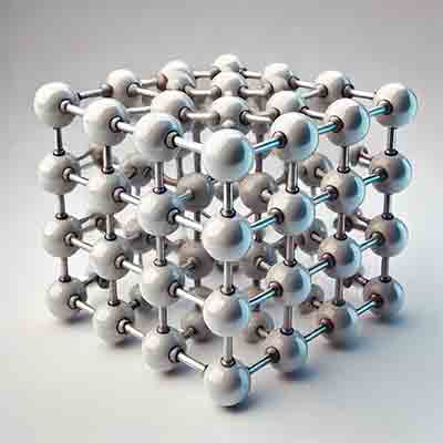
Cubic crystal substrates are wafer materials whose atoms are arranged in a highly symmetrical cubic lattice. In semiconductor research, this crystal structure is important because it affects electron mobility, bandgap behavior, lattice matching, epitaxial growth, and overall device performance.
Many important semiconductor wafers, including silicon, germanium, gallium arsenide, and indium phosphide, are based on cubic crystal structures.
Why Cubic Crystal Structure Matters
The symmetry of a cubic crystal helps create predictable electrical, optical, and mechanical behavior. This is especially important when researchers grow thin films, fabricate devices, or study lattice-matched semiconductor heterostructures.
- Supports uniform electronic behavior in multiple crystal directions
- Helps simplify wafer orientation and device fabrication
- Provides well-defined crystal planes such as (100), (110), and (111)
- Improves compatibility with epitaxial thin-film growth
- Affects band structure, carrier mobility, and optical response
Common Cubic Semiconductor Structures
Diamond Cubic
Diamond cubic is the crystal structure found in elemental semiconductors such as silicon and germanium. Each atom is tetrahedrally bonded to four neighboring atoms, creating a strong and highly ordered crystal lattice that is ideal for integrated circuits, MEMS, sensors, and photonics.
Zinc Blende
Zinc blende is a cubic structure common in III-V compound semiconductors. Unlike diamond cubic materials, zinc blende crystals contain two different elements arranged in alternating lattice positions. Examples include GaAs, InP, and some forms of cubic GaN.
Is Indium Phosphide a Cubic Crystal?
Yes. Indium phosphide (InP) is a III-V compound semiconductor with a zinc blende cubic crystal structure. In this structure, indium and phosphorus atoms alternate through the lattice, and each atom is tetrahedrally bonded to four atoms of the opposite type.
InP is especially valuable because it has a direct bandgap, high electron mobility, and strong performance in high-frequency and optoelectronic devices. It is commonly used for lasers, photodiodes, high-speed transistors, fiber-optic communications, and advanced semiconductor research.
What Does [111A] and [111B] Mean?
For polar III-V materials such as InP, the [111A] and [111B] designations describe different polar crystal faces. In general, the A face is associated with the group III element face, such as indium, while the B face is associated with the group V element face, such as phosphorus.
This distinction matters because surface chemistry, etching behavior, epitaxial growth, and thin-film quality can differ between A-face and B-face wafers.
Examples of Cubic Crystal Wafers
Applications of Cubic Crystal Substrates
Cubic crystal wafers are used in many areas of semiconductor and materials science, including:
- Molecular beam epitaxy (MBE)
- Metalorganic chemical vapor deposition (MOCVD)
- Optoelectronic devices
- High-speed transistors
- Photodetectors and laser diodes
- Solar cells and multijunction devices
- Quantum wells and low-dimensional structures
- Electronic, optical, and magnetic thin-film research
UniversityWafer supplies cubic crystal semiconductor substrates for universities, national labs, and device manufacturers researching advanced electronics, photonics, epitaxy, and next-generation semiconductor devices.
