Can you give me quotes on 1 InGaAs wafer as I will be doing experimental work on it for thermophotovoltaic related experiments? I would need very basic cell that does not cost too much as the solar cell will be used in a thermophotovoltaic structure to output electric power with a seperate structure called absorber-emitter layer to change the incoming heat source to NIR region.
Indium Gallium Arsenide (InGaAs) Wafers
InGaAs Substrate for Thermophotovltaic Structure
A solar cell researcher requested the following quote:
Reference #263615 for specs and pricing
Get Your Quote FAST! Or, Buy Online and Start Researching Today!
Video: Learn About InGaAs Image Sensors
InGaAs Substrates for Temperature-Dependent Photoluminescence Measurements
A senior applications scientist requested a quote for the following:
I need the materials for doing temperature-dependent Photoluminescence measurements (room temp down to 10K), to measure the bandgap shifts. I
want to study 2-3 materials with slightly different but known composition.
InGaAs (standard and strained) is one suggestion, but am open to other ideas.
Broken pieces or scrap materials are fine, as long as the composition is known.
Reference #91295 for specs and pricing.
InGaAs Film on Silicon
A corporate scientist requested the following quote:
Reference #223119 for specs and pricing.
What is Indium Gallium Arsenide Applications?
Indium gallium arsenide (InGaAs) is a compound semiconductor material that is 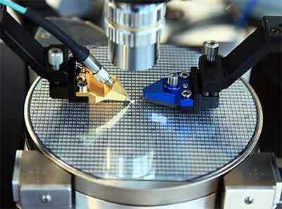 widely used in electronics and photonics applications. It is a ternary alloy made up of indium (In), gallium (Ga), and arsenic (As), and is commonly used as a substitute for silicon in high-speed electronic devices and for certain types of infrared detectors.
InGaAs has several unique properties that make it an attractive material for use in electronic devices. It has a high electron mobility, which means that electrons can move quickly through the material, leading to high-speed device performance. In addition, InGaAs has a direct bandgap, which makes it an ideal material for use in optoelectronic devices such as photodetectors and lasers.
InGaAs is also widely used in the fabrication of high-speed transistors, as well as in the production of infrared detectors for use in night vision and other applications where detection of infrared radiation is necessary. Its unique properties make it an important material in the field of semiconductor technology, and its versatility has led to its use in a wide range of applications.
Overall, InGaAs is an important compound semiconductor material that has played a crucial role in advancing electronic and photonic technologies, and it is likely to continue to be an important material for years to come.
What is a InGaAs Camera?
An InGaAs camera is a type of camera that uses an InGaAs sensor to detect near-infrared light. InGaAs cameras are commonly used in scientific and industrial applications where traditional cameras cannot detect the desired wavelengths of light.
InGaAs cameras are able to detect wavelengths of light in the near-infrared range, typically between 900 and 1700 nanometers. This makes them useful for applications such as thermal imaging, spectroscopy, and night vision, where detection of infrared radiation is necessary.
One of the main advantages of InGaAs cameras is their sensitivity to low levels of light. This sensitivity allows them to detect light that is not visible to the human eye, making them useful for a wide range of applications where traditional cameras would not be effective.
InGaAs cameras are also able to operate at high speeds, making them useful for applications where high frame rates are necessary. They are often used in scientific research, where they are used to capture high-speed images of biological and chemical processes.
Overall, InGaAs cameras are an important tool for scientific and industrial applications where detection of near-infrared light is necessary. Their unique capabilities make them an important asset in fields such as materials science, biological research, and astronomy.
What is InGaAs Detector?
An InGaAs detector is a type of photodetector that is used to detect near-infrared light. It is made up of an InGaAs semiconductor material that is capable of absorbing light in the near-infrared range.
InGaAs detectors are commonly used in scientific, industrial, and military applications where detection of infrared radiation is necessary. They are particularly useful in applications such as spectroscopy, telecommunications, and environmental monitoring.
One of the main advantages of InGaAs detectors is their high sensitivity to low levels of light. They are able to detect light in the near-infrared range with high accuracy, making them useful for a wide range of applications where traditional detectors would not be effective.
InGaAs detectors also have a fast response time, allowing them to quickly detect changes in the intensity of the incoming light. This makes them useful for applications such as laser power monitoring and high-speed optical communication.
Overall, InGaAs detectors are an important tool for a wide range of scientific, industrial, and military applications. Their high sensitivity, fast response time, and ability to detect near-infrared light make them a valuable asset in fields such as materials science, environmental monitoring, and telecommunications.
What is InGaAs Photodiode?
An InGaAs photodiode is a type of semiconductor device that is used to detect light in the near-infrared range. It is made up of an InGaAs material that is capable of absorbing light in the near-infrared region.
InGaAs photodiodes are commonly used in applications where detection of near-infrared light is necessary, such as in telecommunications, spectroscopy, and environmental monitoring. They are also used in medical imaging and security applications.
One of the main advantages of InGaAs photodiodes is their high sensitivity to low levels of light. They are able to detect light in the near-infrared range with high accuracy, making them useful for a wide range of applications where traditional photodiodes would not be effective.
InGaAs photodiodes also have a fast response time, allowing them to quickly detect changes in the intensity of the incoming light. This makes them useful for applications such as optical communication, where high-speed detection is necessary.
Overall, InGaAs photodiodes are an important tool for a wide range of scientific, industrial, and medical applications. Their high sensitivity, fast response time, and ability to detect near-infrared light make them a valuable asset in fields such as materials science, environmental monitoring, and telecommunications.
What is InGaAs Bandgap?
The InGaAs bandgap refers to the energy difference between the valence band and the conduction band in the InGaAs semiconductor material. The bandgap of InGaAs can be tuned by adjusting the ratio of indium (In) and gallium (Ga) in the material, allowing for control over its electronic and optoelectronic properties.
InGaAs has a direct bandgap, meaning that electrons can easily transition from the valence band to the conduction band by absorbing energy from incident photons. The bandgap energy of InGaAs depends on the composition of the alloy, with higher indium content leading to a smaller bandgap and lower energy required for electron excitation.
InGaAs bandgap engineering is an important area of research, as it allows for the optimization of the material's properties for various applications. For example, InGaAs with a small bandgap is suitable for photodetectors and solar cells, while InGaAs with a larger bandgap is suitable for high-speed transistors and lasers.
Overall, the ability to tune the InGaAs bandgap through alloy composition is an important aspect of its versatility and usefulness in electronic and optoelectronic applications.
What is an InGaAS Sensor?
InGaAs sensor refers to a type of image sensor that is based on Indium Gallium Arsenide (InGaAs) semiconductor material. These sensors are designed to operate in the near-infrared (NIR) spectral region, typically from 0.9 to 1.7 micrometers, which is beyond the range of human vision.
InGaAs sensors are commonly used in various applications that require high sensitivity and resolution in the NIR region, such as in industrial inspection, biomedical imaging, and surveillance. They offer several advantages over other types of image sensors, such as high quantum efficiency, low noise, and fast response time.
InGaAs sensors are typically fabricated using a planar processing technique, where a thin InGaAs layer is deposited on a substrate and patterned into an array of pixels. The pixels are then connected to readout electronics, which convert the incoming light signal into a digital image.
Overall, InGaAs sensors are an important technology in the field of imaging and sensing, enabling a wide range of applications that require high sensitivity and resolution in the NIR region.
What is InGaAs Lattice Matched to InP?
InGaAs is a semiconductor material composed of indium (In), gallium (Ga), and arsenic (As). When InGaAs is lattice-matched to InP (indium phosphide) substrate, it means that the crystal structure of the InGaAs layer is perfectly aligned with that of the InP substrate, resulting in very little strain or distortion at the interface between the two materials.
Lattice matching is important in semiconductor device fabrication because it helps to reduce defects and improve the overall quality of the material. In the case of InGaAs/InP, the lattice mismatch between InGaAs and InP is relatively small, which allows for the growth of high-quality InGaAs layers on InP substrates.
InGaAs/InP materials are widely used in the fabrication of various electronic and optoelectronic devices, such as high-speed transistors, photodetectors, and laser diodes. The lattice matching between InGaAs and InP enables the formation of a high-quality heterostructure, which can improve the performance and reliability of these devices.
What are InGaAs Semiconductors?
InGaAs (indium gallium arsenide) is a type of semiconductor material that is composed of indium, gallium, and arsenic. It is a ternary compound semiconductor, meaning it is made up of three elements.
InGaAs is a popular material for a variety of electronic and optoelectronic applications due to its high electron mobility, high carrier concentration, and direct bandgap, which allows for efficient light emission and detection. InGaAs is particularly well-suited for applications in the near-infrared (NIR) region of the electromagnetic spectrum, where its direct bandgap enables efficient absorption and emission of light.
InGaAs semiconductors are used in a wide range of devices, including high-speed transistors, photodetectors, and laser diodes. InGaAs-based photodetectors are commonly used in applications such as fiber optic communication, sensing, and imaging, while InGaAs-based laser diodes are used in applications such as spectroscopy, medical diagnostics, and telecommunications.
Overall, InGaAs is an important semiconductor material that enables a wide range of electronic and optoelectronic devices that operate in the NIR region of the spectrum, and it continues to be an active area of research and development in the semiconductor industry.
InGaAs Ioffe refers to a type of semiconductor material that is composed of indium (In), gallium (Ga), and arsenic (As), and is named after the Russian physicist Abram Ioffe. It is a type of III-V compound semiconductor, which is widely used in the fabrication of various electronic and optoelectronic devices.
The InGaAs Ioffe material is typically used in applications that require high performance in the near-infrared (NIR) region of the electromagnetic spectrum, such as in optical communication, sensing, and imaging. This is because InGaAs has a direct bandgap, which enables efficient absorption and emission of light in the NIR region.
InGaAs Ioffe material is also known for its high electron mobility, which makes it suitable for high-speed transistor applications. In addition, InGaAs Ioffe-based photodetectors are widely used in applications such as fiber optic communication and sensing, while InGaAs Ioffe-based laser diodes are used in applications such as spectroscopy and medical diagnostics.
Overall, InGaAs Ioffe is an important semiconductor material that enables a wide range of electronic and optoelectronic devices, and it continues to be an active area of research and development in the semiconductor industry.
What is the spectral range of InGaAs?
The spectral range of InGaAs (indium gallium arsenide) refers to the range of wavelengths of light that the material can efficiently detect or emit. InGaAs has a direct bandgap that enables it to operate efficiently in the near-infrared (NIR) region of the electromagnetic spectrum.
The spectral range of InGaAs typically covers wavelengths from around 900 nanometers (nm) to 1700 nm, although the exact range can vary depending on the specific composition and fabrication process of the InGaAs material. This makes InGaAs well-suited for applications that require sensitivity in the NIR region, such as fiber optic communication, sensing, and imaging.
In addition to its spectral range, InGaAs also offers high quantum efficiency, low noise, and fast response time, making it a popular choice for various optoelectronic devices. InGaAs-based photodetectors are commonly used in applications such as remote sensing, biomedical imaging, and surveillance, while InGaAs-based laser diodes are used in applications such as telecommunications, spectroscopy, and military applications.
Overall, the spectral range of InGaAs in the NIR region is an important factor that enables a wide range of electronic and optoelectronic devices that operate efficiently in this wavelength range.
What is the Spectral Sensitivity of InGaAs?
The spectral sensitivity of InGaAs (indium gallium arsenide) refers to the material's ability to detect or respond to different wavelengths of light in the near-infrared (NIR) region of the electromagnetic spectrum.
InGaAs has a high sensitivity to light in the 900-1700 nanometer (nm) wavelength range, which is the typical range of the NIR region. The spectral sensitivity of InGaAs is due to its direct bandgap, which enables efficient absorption and emission of light in this wavelength range.
The spectral sensitivity of InGaAs can be further improved by adjusting the composition of the material, such as the ratio of indium to gallium, or by using different growth techniques to reduce defects and improve the crystal quality.
InGaAs-based photodetectors are commonly used in a wide range of applications that require high sensitivity in the NIR region, such as fiber optic communication, remote sensing, biomedical imaging, and surveillance. InGaAs-based laser diodes are also widely used in various applications that require emission in the NIR region, such as telecommunications, spectroscopy, and military applications.
Overall, the spectral sensitivity of InGaAs in the NIR region is an important factor that enables a wide range of electronic and optoelectronic devices that operate efficiently in this wavelength range.
What is the work function of InGaAs?
The work function of InGaAs (indium gallium arsenide) refers to the minimum energy required to remove an electron from the surface of the material and bring it to a point at infinity. In other words, it is a measure of the ease with which electrons can be emitted from the surface of the material.
The work function of InGaAs can vary depending on the specific composition and surface preparation of the material, as well as the method of measurement. However, it is typically in the range of 4.8 to 5.2 electron volts (eV).
The work function of InGaAs is an important parameter that determines the performance of various electronic and optoelectronic devices based on this material. For example, the work function of InGaAs can affect the performance of metal contacts in transistors, photodiodes, and other electronic devices. It can also affect the efficiency of electron injection and extraction in light-emitting diodes and laser diodes.
Overall, the work function of InGaAs is an important material parameter that influences the performance of various electronic and optoelectronic devices based on this material.
InGaAs to Design Optical Waveguide
A Ph.D candidate requested the following quote:
We are looking for InP/InGaAsP wafers (lattice matched). Attached is the
design layout we have in mind. Our purpose here is to design optical
waveguide where the light is confined mostly in the core region (InGaAsP)
sandwiched by the InP cladding layers:
About the wafers:
- Wafer #1 for passive application (no free carriers)
- Wafer #2 option (1) for active application using InP (p+) cap layer
- Wafer #2 option (2) for active application using InGaAs (p+) cap layer
Question on wafer #2 design:
Which one is better for active application? wafer 2 option (1) or option
(2)?
The one with InGaAs (p+) cap layer has better ohmic contact due less
resistance. However, the InGaAs cap layer is absorptive at 1.55um if
designed under lattice matched condition (please confirm). This is partly
the reason why I increased the upper cladding thickness to 450nm and reduce
the InGaAs layer thickness to 50nm in wafer (2). This is done so that the
light in the core can be isolated better from the cap layer.
Please kindly advice.
Lastly, please also advice on the pricing for:
- 2 piece of wafer #1
- 1 piece of wafer #2
Reference #162325 for specs and pricing.