Fabricate Dielectric Metasurfaces with GaP Wafers
A PhD candidate researching AI and robotics requested a quote for the following Gallium Phosphide substrate.
I am interested in purchasing a wafer with the following specifications:
- Substrate: Si/SiO₂/GaP
- Wafer size: 3 or 4 inches (either size is acceptable)
- SiO₂ layer thickness: 1 µm
- GaP layer thickness: 110 nm
- Si wafer thickness ~575 µm
I would prefer the method that yields the highest quality GaP. The conductivity and crystal orientation of the silicon substrate are not critical for my application.
I am trying to make dielectric metasurfaces with GaP for photonic applications.
Reference #323520 for specs and pricing.
Get Your Quote FAST! Buy Substrates Online and Start Researching Today!
What is Dielectric Metasurfaces?
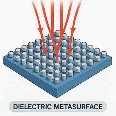
A dielectric metasurface is a type of artificially engineered material made from an array of tiny, carefully arranged dielectric (non-conducting) structures—usually on the subwavelength scale—that can control and manipulate electromagnetic waves in ways not possible with natural materials.
Here’s a breakdown:
1. Basic Concept
-
A metasurface is a 2D version of a metamaterial: it’s a thin layer patterned with nanoscale  features that modify how light interacts with it.
-
In a dielectric metasurface, those features are made of high-refractive-index dielectric materials (like silicon, titanium dioxide, or gallium nitride) instead of metals.
2. Why Dielectric Instead of Metallic?
-
Metallic (plasmonic) metasurfaces suffer from high optical losses due to absorption.
-
Dielectric metasurfaces avoid those losses, allowing for high efficiency and low heat dissipation. They rely on Mie resonances (resonances of light within the dielectric nanostructures) to achieve the desired control.
3. Capabilities
Dielectric metasurfaces can manipulate key properties of light:
-
Phase: bend or focus light like a lens, but in an ultrathin form.
-
Amplitude: control intensity transmission or reflection.
-
Polarization: convert linear to circular polarization or rotate polarization.
-
Wavelength selectivity: act as filters.
4. Applications
-
Flat optics: replacing bulky lenses with flat, nanostructured surfaces (e.g., “metalenses”).
-
Beam steering: for LiDAR, AR/VR, and optical communication.
-
Holography: creating highly efficient 3D holograms.
-
Sensing: detecting gases, biomolecules, or temperature changes via resonance shifts.
-
Quantum photonics: controlling single photons in integrated optical circuits.
👉 In short: Dielectric metasurfaces are ultrathin optical elements made from nanoscale dielectric structures that shape light with high efficiency, enabling flat and compact alternatives to traditional bulky optical components.

 features that modify how light interacts with it.