
We are interested in purchasing some silicon nitride wafers for photonics applications, I have a few questions: What is the SiO2 BOX thickness for the wafers listed on your nitride on silicon page ? What is the nominal refractive index of the SiN in the visible (~600 nm) for the “standard”, “low”, and “super low” stress films. Can you do runs of a custom SiN thickness? Say around 250 nm? Would you recommend a particular stress type (standard/low/super low) for visible photonic waveguide applications?
SiN Substrates for Photonics Applications
A PhD scientist researching Photonic Waveguides requested a quote for the following.
Reference #312613 for specs and pricing.
Get Your Silicon Wafer Quote FAST! Or, Buy Online and Start Researching Today!
Substrates for Photonic Applications
Scientist:
I am interested in purchasing 3 inch wafers of ~330nm SiN on ~3300nm SiO2 all on Si substrate, for photonic applications. If there are wafers in stock that are suitable for photonic/waveguide applications but not of the exact thickness mentioned above, I can also take those because that will arrive sooner.
Silicon Nitride Used to Fabricate SiN Waveguides
Pls see below for the offer on required "330nm SiN / 3um SiO2 / Si stack" Wafer for photonic applications,We also quote 4'' for your reference
1. 3'' Waveguide Layer: Si3N4 0.33um grown LPCVD
Insulating Layer: Thermal Oxide SiO2 3.0um
Substrate Carrier Layer: <100> orient. Dia. 76.2+/-0.3mm,380+/-25um,SSP or DSP,N or P-type,1~100 Ohm.cm,Semi flat
Stack Structure: 330nm Si3N4 / 3000nm SiO2 / 380um Silicon Wafer
Qty. 10pcs
2. 4'' Waveguide Layer: Si3N4 0.33um grown LPCVD
Insulating Layer: Thermal Oxide SiO2 3.0um
Substrate Carrier Layer: <100> orient. Dia. 100.0+/-0.3mm,500+/-25um,SSP or DSP,N or P-type,1~100 Ohm.cm,Semi flat
Stack Structure: 330nm Si3N4 / 3000nm SiO2 / 500um Silicon Wafer
Reference #266490 for pricing.
How Large is the Photonics Market?
Photonics research is of great econmic performance. Thousands of companies are currently developing and relying on photonic technologies. Currently the global market size of Key Enabling Technologies (KEY) is worth over $900 billion!
KEY Valuations by Market Segement
- Photonics Greater than $355 Billion
- Micro and Nano-Electronics: Greater than $250 Billion
- Advanced Manufacturing: Greater than $150 Billion
- Biotechnology: Greater than $92 Billion
- Nanotechnology: Greater than $20 Billion
SiO2 Substrates To Fabricate Integrated Photonic Circuit
A PhD candidate requested a quote for the following.
I am loooking for Si on SiO2 wafers for the fabrication of an integrated photonic circuit. For this, I ideally need the following specifications: - Si-thickness: 220 nm (or custom values between 200 and 250 nm if possible) - BOX/SiO2-thickness: 1.8 microns (or other custom value between 1.7 and 2.4 microns if possible) - low defect density( high crystallinity of Si-layer - low surface roughness of Si-layer to avoid surface scattering From your inventory list, the wafer with SOI ID#3381 seems to be the best fit.
Question:
Can you elaborate on what Grade = 'Prime' means? And do you also have other Si-layer-thicknesses in stock?
Answer:
"Prime grade" refers to the highest quality standard for silicon wafers, primarily in terms of surface quality, flatness, and defect level. Prime-grade wafers are typically used in high-performance applications, such as in integrated circuit (IC) manufacturing, where minimal defects and high uniformity are critical.
Here are some key characteristics of prime-grade silicon wafers:
- Surface Quality: Prime wafers have a polished, mirror-like surface with extremely low levels of surface roughness, scratches, or contamination.
- Flatness: They have very tight tolerances for flatness, often with specifications for total thickness variation (TTV) and bow/warp control, to ensure uniformity across the wafer surface.
- Defect Density: Prime wafers have a very low defect density, meaning minimal particle contamination, crystalline defects, or impurities.
- Edge Quality: Prime wafers undergo edge profiling to reduce chipping, which is crucial for handling and preventing defects during processing.
Prime-grade wafers contrast with lower grades, such as test or mechanical grades, which are used for less critical applications like testing equipment or calibration, where
Reference #317847 for specs and pricing.
Revolutionizing Photonics: Top Silicon Wafers for Advanced Applications
Silicon wafers are the foundation of photonics, powering high-speed data transmission and cutting-edge sensing technologies. These tiny marvels enable breakthroughs in telecommunications, healthcare, and quantum computing. Let's explore the exciting world of top silicon wafers for photonics applications and see how they're shaping our technological future, changing how we work with light and information at a basic level.
Key Takeaways
- Silicon wafers are essential components in photonic devices, manipulating light at the microscopic level
- Highly doped, Silicon-on-Insulator (SOI), and standard silicon wafers are key types used in photonics
- Ultra-high purity, precise thickness control, and smooth surfaces are crucial features for photonic applications
- Silicon wafers enable advancements in optical communications, sensors, quantum computing, and lidar systems
- The manufacturing process involves crystal growth, slicing, lapping, etching, and polishing stages
- Ongoing research aims to overcome challenges in light emission, heat management, and integration with electronics
Understanding Silicon Wafers in Photonics
Silicon wafers are thin slices of crystalline silicon that form the base for many photonic devices. They're great for controlling light at tiny scales, which is useful for optical communications, sensing, and computing. The crystal structure of silicon is perfect for guiding light waves, allowing the creation of complex photonic circuits that can process information at light speed.
The magic of silicon wafers is in how they guide and control light super precisely. Photonic applications use these wafers to make tiny structures that can control light signals, similar to how electronic circuits control electrical signals. This works because silicon has special optical properties, like how it bends light and doesn't absorb much in the near-infrared range, which is important for telecommunications. By etching really small patterns onto silicon wafers, engineers can make waveguides, resonators, and other photonic parts that are the building blocks of advanced optical systems.
Types of Silicon Wafers for Photonics
There are different types of silicon wafers for photonics, each with special properties for specific uses in optoelectronics:
1. Highly Doped Silicon Wafers
Highly doped silicon wafers are the workhorses of photonic devices. They have extra atoms added to their structure, which changes how they interact with light and electricity. This process, called doping, involves adding impurities like boron or phosphorus to the silicon, which alters its electrical and optical properties.
These wafers are great for making lasers and sensors. They can carry more electricity and interact with light in special ways, which is important for many photonic devices. The high doping levels allow for efficient photodetectors, modulators, and even light-emitting devices when combined with other materials. Being able to adjust the electrical properties of silicon through doping opens up many possibilities for combining electronic and photonic functions on one chip.
2. Silicon-on-Insulator (SOI) Wafers
Silicon-on-Insulator (SOI) wafers are like sandwich cookies for photonics. They have a thin layer of silicon on top of an insulating material, usually silicon dioxide. This special structure helps control light really well, which is perfect for making tiny optical circuits. The insulating layer stops light from escaping into the base, allowing for very efficient waveguides and other photonic structures.
SOI wafers are used in cool devices like super-fast optical switches and sensors that can detect tiny changes around them. They're important for making photonic devices smaller and more efficient. The unique structure of SOI wafers allows for high-contrast waveguides, which can tightly control light and make photonic circuits smaller. This technology is crucial for developing integrated photonic chips that can handle both optical and electrical signals, paving the way for next-generation computing and communication systems.
3. Standard Silicon Wafers
Standard silicon wafers might sound basic, but they're the workhorses of the photonics world. These wafers come in different sizes and thicknesses, making them useful for various applications. The purity and perfect crystal structure of standard silicon wafers make them a great starting point for many photonic devices.
Standard silicon wafers are often used as a starting point for creating more complex photonic structures. They're like a blank canvas for scientists and engineers to create their photonic masterpieces. These wafers can be processed using many techniques, like photolithography, etching, and deposition, to create intricate photonic structures. They work well with existing semiconductor manufacturing processes, making them good for large-scale production of photonic devices, which helps bring photonics into mainstream technology.
Key Features of Top Silicon Wafers for Photonics
What makes a silicon wafer great for photonics? Let's look at the important characteristics that allow these wafers to excel in photonic applications:
Key Features of Silicon Wafers for Photonics
- Ultra-high purity silicon (99.999% or higher) is essential for optimal optical performance
- Precise thickness control, typically ranging from 300 to 700 micrometers, enables specific photonic applications
- Extremely smooth surface with roughness less than 1 nanometer minimizes light scattering
- Crystal orientation, usually <100>, affects optical and electronic properties
- Low defect density (less than 1 defect per square centimeter) ensures uniform optical behavior
- High transmission in near-infrared wavelengths (90-95% for 700nm-3μm) makes silicon ideal for telecom applications
- Compatibility with existing semiconductor manufacturing processes allows for cost-effective production
- Ability to integrate electronic and photonic components on a single chip enables advanced device designs
- Thermal stability up to 1000°C supports high-power optical applications
- Customizable doping levels allow fine-tuning of electrical and optical properties
These features are crucial for creating photonic devices that can manipulate light with incredible precision. The purer and smoother the wafer, the better it can guide light without losing signal strength. The ultra-high purity ensures that light can travel through the silicon with minimal absorption or scattering, which is essential for maintaining signal integrity in photonic circuits. The precise thickness control allows engineers to design devices that operate at specific wavelengths, crucial for applications like wavelength division multiplexing in optical communications.
The extremely smooth surface is particularly important as it reduces light scattering at interfaces, improving the efficiency of photonic devices. The crystal orientation affects how light interacts with the silicon lattice, influencing properties such as birefringence and nonlinear optical effects. Low defect density is critical for ensuring uniform optical behavior across the entire wafer, which is essential for producing consistent and reliable photonic devices at scale.
Applications of Silicon Wafers in Photonics
Silicon wafers are behind many technologies we use every day. Let's explore some exciting ways these wafers are used in photonics, changing various industries and enabling new technological capabilities:
1. Optical Communications
Silicon wafers are key in optical communication systems. They're used to make tiny devices called optical modulators, which can turn electrical signals into light signals very quickly. This technology lets us send huge amounts of data through fiber optic cables across the world. Silicon photonics enables integrated optical transceivers that can handle data rates of hundreds of gigabits per second, much faster than traditional electronic systems.
Silicon wafers are also used to create other important parts of optical communication systems, like wavelength multiplexers, optical switches, and photodetectors. These integrated photonic circuits are driving the development of next-generation data centers and telecommunications networks, meeting the growing demand for bandwidth in our connected world.
2. Sensors and Detectors
Photonic sensors made with silicon wafers can detect many things, from chemicals in the air to tiny movements. These sensors are used in environmental monitoring and medical devices that can detect diseases early. The high sensitivity and integration capabilities of silicon photonics allow for compact, highly accurate sensing devices.
For example, silicon photonic biosensors can detect specific molecules very sensitively, enabling fast and accurate medical diagnoses. In environmental monitoring, silicon-based optical sensors can measure air and water quality very precisely. The ability to integrate these sensors with electronic readout circuits on the same chip allows for smart, networked sensing systems that can provide real-time data for various applications.
3. Quantum Computing
The strange world of quantum computing also uses silicon wafers. Scientists are using these wafers to create quantum bits, or qubits, which could lead to computers that are much faster than anything we have today. Silicon's long coherence times and compatibility with existing semiconductor manufacturing processes make it good for scaling up quantum computing systems.
Researchers are exploring different ways to create silicon-based qubits, including using the spin of individual electrons in silicon quantum dots or the nuclear spins of phosphorus atoms placed in silicon. The ability to precisely control and manipulate these quantum states using integrated photonic circuits opens up new possibilities for quantum information processing and quantum communication systems.
4. Lidar Systems
Lidar, which stands for Light Detection and Ranging, uses laser light to measure distances. Silicon wafers are used to make the tiny mirrors and sensors in lidar systems, which are important for things like self-driving cars and 3D mapping. Silicon photonics enables compact, high-performance lidar systems that can quickly scan the environment with high resolution.
Advanced silicon photonic lidar systems can include beam-steering capabilities, allowing for fast and precise scanning without moving parts. This technology is not only changing autonomous vehicles but also finding uses in robotics, augmented reality, and industrial automation. The ability to integrate lidar sensors with processing electronics on a single chip is driving the development of smarter and more responsive sensing systems.
Manufacturing Process of Top Silicon Wafers
Creating high-quality silicon wafers for photonics is like baking a really complicated cake. Here's a simplified version of how it's done, with each step carefully controlled to ensure the highest quality and consistency:
1. Crystal Growth: It starts with very pure silicon that's melted and slowly cooled to form a big crystal cylinder called an ingot. This process, called the Czochralski method, involves carefully controlling the temperature and rotation of the growing crystal to ensure uniform properties throughout. The resulting single-crystal ingot can be up to 300mm wide and over a meter long.
2. Slicing: The ingot is then cut into thin wafers, like slicing bread, but much more precisely. Wire saws with diamond-coated wires cut the ingot into wafers as thin as 200 micrometers. This step needs to be very precise to avoid damaging the crystal structure and ensure the wafers are all the same thickness.
3. Lapping: The wafers are smoothed out to make them flat and the right thickness. This uses a mix of abrasive particles to remove tiny bumps from the wafer surface. Lapping helps achieve the exact thickness needed for specific photonic applications and prepares the surface for further processing.
4. Etching: A special chemical bath removes any damage from the slicing process. This step uses a mix of acids or bases to dissolve a thin layer from the wafer surface, removing any leftover damage from the mechanical processes. Etching also helps reveal the pure crystal structure of the silicon, which is essential for its optical properties.
5. Polishing: Finally, the wafers are polished to a mirror-like finish, making them ready for photonic applications. Chemical-mechanical polishing (CMP) is used to achieve an ultra-smooth surface with roughness on the order of angstroms. This final step is crucial for minimizing light scattering and ensuring optimal performance in photonic devices.
Each of these steps is carefully controlled and monitored to ensure the highest quality wafers for photonic applications. Advanced measurement techniques are used throughout the process to check the wafer's properties, including thickness uniformity, surface smoothness, and crystal perfection. The entire manufacturing process takes place in ultra-clean environments to prevent contamination that could affect the wafer's optical and electrical properties.
Challenges and Future Trends
While silicon wafers have revolutionized photonics, there are still some challenges to overcome. Researchers and engineers are working on solutions to push the boundaries of what's possible with silicon photonics:
1. Light Emission
Silicon isn't great at emitting light on its own due to its indirect bandgap. Scientists are working on ways to add other materials to silicon or change its structure to make it better at producing light. Some promising approaches include:
- Integrating III-V semiconductors like indium phosphide with silicon to create efficient light sources
- Exploring germanium-on-silicon structures for light emission in the near-infrared spectrum
- Developing silicon nanostructures that enhance light emission through quantum confinement effects
- Investigating rare-earth doping of silicon to create silicon-based lasers
These advancements could lead to fully integrated silicon photonic circuits that include light sources, modulators, and detectors all on a single chip.
2. Heat Management
As photonic devices get smaller and more powerful, managing heat becomes a big challenge. The high optical power densities in compact photonic circuits can lead to thermal issues that affect device performance and reliability. Researchers are developing new ways to keep these tiny devices cool, including:
- Advanced thermal management materials and structures integrated into silicon photonic chips
- Novel device designs that minimize heat generation and improve heat dissipation
- Active cooling techniques tailored for integrated photonic circuits
- Exploring the use of two-dimensional materials like graphene for heat spreading in photonic devices
Effective heat management is crucial for enabling high-performance, densely integrated photonic systems that can operate reliably in various applications.
3. Integration with Electronics
One of the big goals is to combine photonic and electronic components on the same chip. This could lead to computers that use both light and electricity to process information, making them much faster and more efficient. Challenges in this area include:
- Developing manufacturing processes that are compatible with both electronic and photonic components
- Creating efficient interfaces between optical and electrical domains
- Optimizing chip designs to minimize crosstalk between electronic and photonic elements
- Developing new materials and structures that can serve both electronic and photonic functions
Successful integration of electronics and photonics could revolutionize computing, enabling new architectures for artificial intelligence, high-performance computing, and ultra-fast data processing.
The future of silicon wafers in photonics looks bright. Scientists are exploring new materials and structures to make even better photonic devices. For example, Silicon High Electron Mobility Transistors (HEMTs) are pushing the boundaries of what's possible in high-speed electronic and photonic circuits. These advanced transistor structures combine the benefits of silicon with high-mobility channel materials, enabling faster switching speeds and improved performance in both electronic and photonic applications.
Other exciting trends in silicon photonics include:
- Development of on-chip optical frequency combs for applications in spectroscopy and precision measurement
- Exploration of nonlinear optical effects in silicon for all-optical signal processing
- Integration of plasmonic structures with silicon photonics to enhance light-matter interactions at the nanoscale
- Advancements in silicon photonic packaging and testing to enable large-scale production and deployment of photonic systems
Conclusion
Silicon wafers are the unsung heroes of the photonics revolution. From enabling super-fast internet connections to powering cutting-edge sensors and quantum computers, these tiny slices of silicon are shaping our technological future in amazing ways. The special properties of silicon, combined with years of manufacturing know-how from the semiconductor industry, have made silicon photonics a key technology for the 21st century.
As research continues and manufacturing techniques improve, we can expect to see even more amazing applications of silicon wafers in photonics. The ongoing efforts to overcome challenges in light emission, heat management, and integration with electronics are opening up new possibilities for silicon photonic devices. These advancements could lead to transformative technologies such as:
- Ultra-high-bandwidth optical interconnects for next-generation data centers and supercomputers
- Integrated photonic sensors for environmental monitoring, healthcare diagnostics, and industrial process control
- Quantum photonic circuits for secure communication and quantum information processing
- Neuromorphic photonic systems that mimic the human brain's information processing capabilities
- Advanced lidar and imaging systems for autonomous vehicles and augmented reality applications
Whether it's making our communication networks faster, our medical diagnostics more accurate, or our computers more powerful, silicon wafers will be at the heart of these innovations. The integration of photonics with existing electronic technologies promises to unlock new levels of performance and functionality across a wide range of applications.
The world of photonics is moving fast, and silicon wafers are helping to light the way. As we continue to push the boundaries of what's possible with light and silicon, who knows what incredible technologies we'll see in the future? One thing's for sure: silicon wafers will be there, quietly enabling the next big breakthroughs in photonics. From quantum computing to artificial intelligence, from advanced medical diagnostics to space exploration, the impact of silicon photonics will be felt across industries and scientific disciplines, shaping the technological landscape for generations to come.
What Are Some Photonics Applications?
What are some photonics applications? These applications range from medical devices to microwave photonics.
We'll cover:
- Microwave photonics
- Digital baseband communication
- Medical devices
- Synthetic aperture radar
Listed below are some of the more important applications for photonics. In addition, this article will cover some of the newest developments in photonics. For more information, visit our website! Also, be sure to check out our upcoming events!
Microwave photonics
Microwave photonics combines the fields of optics and radiofrequency engineering to  study the interaction between these two technologies. It has the potential to generate, distribute, measure, and process microwave and millimeter-wave signals. The technology uses photonic devices to achieve these functions. Since its inception, microwave photonics has found applications in various fields and is a rapidly developing field. Here are some of the latest applications of microwave photonics.
The book features contributions from leading international researchers on wave generation, detection, control, and propagation. It also explores the components and devices used to implement these technologies, including radio-over-fiber systems, optical transmitters and receivers, and optical switchers. Each chapter explores theories and techniques related to these technologies, and contributors provide insights into future developments. This book will benefit all researchers working in the field of microwave photonics.
The researchers at Texas A&M University have developed a microchip that uses microwave photonics to increase the quality of a microwave signal. The new chip has two distinct advantages over previous solutions: its small size, high-speed operation, and improved performance. Microwave photonics applications are becoming a reality in many areas of technology, from medical imaging to industrial equipment. They're the next wave in photonic technology.
Advanced microwave systems are able to reduce nonlinear crosstalk by as much as 30 dB. With the ability to combine multiple photonic building blocks, these devices can be easily integrated into a single device. This technology is enabling the development of a new field of research. Moreover, it could enable new types of microwave devices. So, it's never too early to start thinking about the applications of microwave photonics.
The advancement of the manufacturing process is making it possible to manufacture integrated photonic components. Several recent European facilities have become available for multi-project wafer production runs. By collaborating with industry, these facilities have made it possible for designers to share the cost of fabrication tools and facilities. As each foundry uses a particular substrate and masters certain components onto it, high-quality photonic components can be produced. And despite the technological advancements in microwave photonics, these devices can still prove challenging to design and implement in a wide range of environments.
Digital Baseband Communication
As the backbone of modern wireless communication systems, photonic networks are increasingly being used to distribute information and make connections. While photonics has many uses in modern society, the growing interest in wireless photonic systems is increasing the need for low-cost, high-performance systems. Two of the most common methods for data transmission in photonic systems are digital baseband and RoF (Radio-over-Fiber) optical communication. Another emerging field, opto-atomics, is the integration of atoms and photonic devices. As the name suggests, photonic applications have a wide range of applications, including accurate time-keeping, communications, and imaging.
Optical transmission performance is compromised by three factors: the short transmission distance, a small launch power, and chromatic dispersion. Although linear DSP algorithms can compensate for chromatic dispersion, frequency chirp and the interplay between them causes a high order distortion. High-order distortion is a common characteristic of optical signals and is the primary cause of deteriorated transmission performance.
The development of ultrahigh-speed photonic systems using millimeter wave or terahertz carriers is also a photonics application. Such systems have already proven superior to conventional RF technologies, although several technical challenges remain. Additionally, practical applications require high-data-rate, wireless-distance communications. However, the future of photonics is looking bright. So, now is the time to start exploring these applications in your field. So, what are the benefits of using photonics for digital baseband communication?
One of the most important applications of photonics is digital baseband communication. This application is crucial for delivering high-quality audio and video. Digital baseband communication is a photonics application that is making its way into the space industry. It has many advantages over conventional methods, and is one of the most common. For one thing, photonics is more convenient than conventional radio. Moreover, it can be used to transfer RF signals.
Besides being cost-effective, photonic radio is capable of high data-rates and connection reliability. It can operate over distances of 400 kilometers and reach up to 1.32 Tbps. The photonic radio architecture demonstrates the general concept of the system and exploits two polarizations of an optical wavelength. It is possible to combine multiple photonic architectures to create a high-performance system.
Medical devices
Implantable Photonic Devices: These devices can monitor health and act as therapeutic tools for many ailments. These devices can be implanted into the body and are often made of thin-film or rigid electronic components. Their uses range from wound treatment to skin rejuvenation. Some photonic devices may also be used for brain-disease therapy or mental health. Photonics are becoming an integral part of modern medical devices.
Medical imaging: Modern imaging technologies have increased the sensitivity and specificity of diagnostic measurements. Imaging for blood glucose and other measurements based on light are made easier thanks to photonic technologies. In addition, the ability to visualize the shape and movement of objects is crucial in the detection of various diseases. With state-of-the-art optical technologies, diagnostic instruments can now perform more precise measurements of blood sugar and lipid levels. Moreover, optical measurements of glomerular filtration rate can replace traditional urine taste tests. Chest X-ray imaging: Chest x-ray images allow doctors to detect lung disease and diagnose other conditions.
Rapid diagnostics: Rapid diagnosis is crucial for major and infectious diseases. It is also becoming possible for patients to perform their own tests at home or in the point of care setting. Photonic ICs are joining the medical device industry, adding value and functionality. So, what are photonics applications in medical devices? If you have any questions about their potential benefits, contact our research team. You can learn more at photonicsapplications.
Medical imaging: Advances in technology and miniaturisation make photonics applications in medical devices possible. This is making it easier for doctors to diagnose diseases and treat patients more efficiently. For patients, the development of medical imaging devices is becoming more affordable, enabling more people to get access to better healthcare. So, do not delay the development of photonics technologies. You never know when the world is going to need them. If you do, you might be the next big thing in medicine.
Endoscopes: Optical fibers are now commonly used for less invasive imaging and surgery of internal organs. Using optical fibers, high-level laser light is delivered to the internal organ and destroys tumors. Other uses of light include photochemical modification of cellular functions and removing tissues through a photothermal or photomechanical process. These technologies have been used in a variety of medical devices, including lasers and ultrasound machines.
Synthetic aperture radar
Synthetic aperture radar (SAR) imaging is one of the most promising applications of photonics in radar. The method of imaging objects using millimeter electromagnetic waves uses concepts developed for radar, but these concepts also apply to other optical and photonic technologies. The hardware behind ISAM is derived from optical coherence tomography, a widely used form of interferometric ranging. The resulting images can have an accuracy of 50 percent to one-half the diameter of the antenna.
The principle of SAR is a simple one: to detect an object from a distance, a fixed antenna must be positioned above the object. The longer the antenna is pointed at an object, the bigger its synthetic aperture is. This process allows for consistent spatial resolution over a wide range of viewing distances. Hence, it can be applied to radar aircraft and spacecraft, where longer ranges of detection are required.
The first successful focussed airborne SAR image was captured at Willow Run Airport in August 1957. The principle was publicly acknowledged in an April 1960 press release. The system consisted of an airborne element, developed by Texas Instruments, a ground data-processing station by WRRC, and a Beech L-23D aircraft. In the early 1960s, NASA began to use synthetic aperture radar in the space shuttle. In 2004, the Cassini mission used the technology to map the surface of Titan, a planet partly hidden in its atmosphere.
The technology behind SAR uses photonics to overcome the problems of electronic solutions. By integrating a photonic integrated circuit into a receiver, the device can be more compact and lower power-consuming than a conventional radar. The SPACEBEAM Project is an international research project to test a spaceborne SAR receiver. It utilizes multiple reconfigurable beams with a hybrid photonic integrated circuit at its core.
Unlike conventional radar systems, SAR uses ultra-short pulses of electromagnetic energy to measure objects. The pulses can change in frequency, so they require an electronics system that can cope with extremely high instantaneous power. This allows a more precise measurement of distance and resolution. The system has been used in numerous applications since the 1960s. So far, the technology is being widely used in the military.
Video: Photonic Crystal and Their Applications
Recent Advances in Photonic Crystals
Recent advances in photonic crystals have been explored from the perspective of band-gap/defect engineering. The number of explanations is probably insufficient, as space is at a premium. Nonetheless, the author hopes that the reader will gain a sense of the constant progress in fundamental technology, which is enabling light control in tiny volumes. Let us look at some of the recent advances in photonic crystals. The main goals of this article are to describe the fundamental properties of photonic crystals.

What are Optical Fibres?
Optical fibres and photonic crystal are two different classes of light-conducting materials. Optical fibres have hollow or solid cores and are clad in a periodic pattern of microcapillaries. These materials can be used to measure temperature and strain simultaneously, as well as to confine light in hollow cores. These materials are also useful for sensing applications, such as Brillouin scattering.
Optical fibres and photonic crystal are among the most advanced lightguides available. They range in nonlinearity from low-index fibers used in high-power pulses to their highly nonlinear counterparts used for supercontinuum generation. These materials are fabricated with a complex stack-and-draw fabrication process that allows precise control of the core's index properties. As a result, the high-quality optical fibres available today have a large range of applications.
Optical fibers are designed to control the near field of an optical mode along a fiber's length. The polarization of the mode varies depending on the shape of the fiber. The polarization of a injected light must match the polarization of the mode to be propagated. In other words, a fiber must be designed to maintain the optical mode's properties even after the light has been propagated a certain distance.
Optical fibres and photonic crystal fibres are similar in appearance and their fundamental properties. In fact, these two technologies can work together for the same purpose: high-quality transmission and low-cost storage. As a result, optical fibres and photonic crystals are one of the hottest fields in optical research today. They combine the best of both worlds and offer unique advantages and applications. You can use optical fibers for nonlinear devices, high-power transmission, gas sensors, and other advanced applications.
What are Colloidal Crystals?
In a nutshell, colloidal crystals are ordered arrangements of fine-grained colloid particles or molecules with repeating subunits. Examples of colloidal crystals include gem opal, which exhibits a close-packed, locally periodic structure. The bulk properties of a colloidal crystal depend on its composition, particle size, packing arrangement, and degree of regularity. Colloidal crystals have applications in photonics, phase transitions, and self-assembly.
The basic design principle of colloidal photonic crystals is described. Representative examples of sensors for various stimulus are also discussed. Furthermore, the crystals can grow single crystals of a certain size. These advantages enable their widespread use. Aside from being photonic crystals, they are also able to operate without external energy, which makes them useful for a variety of applications. Consequently, colloidal crystals are a powerful tool in photonics.
The origin of colloidal crystals is not clear, but they are considered photonic crystals. The Schiller layers in iron oxide sols and glassy colloidal samples have been found to be the photonic equivalent of crystalline grains. The crystalline forms of tobacco and tomato viruses were first discovered by W.M. Stanley, who used X-ray diffraction to confirm their crystalline structure. As the research on these crystals progressed, they became more common in science and medicine.
The formation of colloidal photonic crystals has recently gained considerable attention. These photonic crystals are periodic assemblies of nanoparticles. This periodicity results in an optical property called the photonic bandgap, similar to an electronic band gap. Consequently, colloidal photonic crystals are a very promising PC material. And the future of colloidal crystals is bright! They are an excellent choice for photonic devices, from the pharmaceutical industry to biomedicine.
What are 2D Photonic Crystals?
A schematic illustration of a 2D photonic crystal shows the unit cell as a metallic cylinder sandwiched between two parallel-plate metals (PBS). The first Brillion zone and the second (TE) band are crossed at the M point. Insets show the corresponding first Brillion zones. A three-dimensional view of the PBS reveals the ring as a closed structure. This technology will revolutionize quantum optics research.
The periodicity of the 2D photonic crystal structure must be larger than half of the wavelength of the light waves inside the material. Visible light has a wavelength of 400 to 700 nanometers. Calculating the wavelength inside a material involves multiplying the wavelength by the average index of refraction. In order to fabricate a two-dimensional photonic crystal, high and low dielectric constant regions must be fabricated on a large scale. To accomplish this, thin-film deposition is routinely used.
Two-dimensional photonic crystals are dielectric materials with spatial periodicity. They have unique properties, making them attractive optical materials. In addition to being effective omni-directional reflectors, 2D photonic crystals can be used as optical filters and colour-changing paints. While 3D photonic crystals are still in their infancy, they have great potential in optical computation. So far, there are two main types of 2D photonic crystals: one-dimensional and two-dimensional.
Two-dimensional photonic crystals can be characterized by a degenerate ring in momentum space. The structure is typically made of a parallel-plate metal or a square array of metallic cylinders. Its z-inversion symmetry is broken by opening an air gap between the metallic cylinders. This breaks symmetry, allowing the TE and TM waves to be correlated. Electromagnetic coupling then results in a complete topological band gap at the degenerate frequency. The resulting topological band gap is known as the Berry phase.
What are Single-Mode Properties?
A typical fiber made of photonic crystals consists of a solid core and a ring of air holes in its cladding region. The guiding properties of these fibers are based on their effective index. A photonic crystal fiber's cladding region is strongly wavelength dependent, and the ratio of the guided mode wavelength to its hole-to-hole distance approaches zero. As the cladding region of a fiber increases in wavelength, its effective index is lowered and the guided mode cutoff condition approaches zero.
In order to study the single-mode properties of a photonic crystal fibre, one must first understand the fundamental theory of optical fibers. A photonic crystal fibre can be classified into two modes: the first mode is guided by its lobes while the second mode is guided by its airholes. Depending on the core size and wavelength, these two modes are guided in different ways. Single-mode fibers may have a larger or smaller hole than other types of optical fibres.
A multimode fiber may be characterized by a high numerical aperture due to its pump cladding. High numerical aperture and narrow hole spacing are possible with pump cladding. Small hole ratios and spacings can enable single-mode guidance over wide wavelength regions. Alternatively, pump cladding can be used for high-numerical-aperture multimode fibers. However, the main challenge of multimode fibers is the calculation of their mode properties.
As the single-mode operation of a fibre is robust, it is possible to test its single mode operation by measuring the reconstructed near-field profile. The LP11 and LP21 contributions are measured at 1064 nm. A zero offset corresponds to the highest intensity of the input beam, and a negative value indicates the lowest power of the output beam. Furthermore, increasing the offset reduces the coupling efficiency of a fibre to the single-mode mode.
What is the Band Gap of Photonic Crystals?
The band gap of photonic crystals is the difference between the frequencies at which the light is absorbed and reflected. A photonic crystal has a band gap when the center frequency of the material is 19THz. This band gap is visible at low frequencies, but it becomes less visible as k increases. The widest bandgap frequency is around 0.8-1.2 GHz, and the frequency at which the band gap disappears is 0.03 GHz.
In the one-dimensional case, a photonic band-gap structure consists of alternating layers of different refractive indices. Such a structure is manufactured using molecular beam epitaxy, chemical vapour deposition, or metallo-organic CVDs. For the two-dimensional version, dry etching with reactive ions can be used. This method has the advantage of enabling nanometre-scale precision, but has a limited depth.
For example, a PX's band gap is determined by its shape. In contrast, an ordinary crystal has an optical band gap that is not entirely complete. A complete band gap allows omnidirectional reflection. This is important for certain applications. In some applications, the band gap may not be completely closed. In these cases, a semiconductor may be doped, allowing it to exhibit complete parallelism between electrons and photons.
Besides the bandgap, photonic crystals also have several other properties that make them useful in optical research. One of these characteristics is the defect mode. This defect mode can control the propagation state of light and suppress spontaneous radiation. A defect mode is also possible in one-dimensional photonic crystals. In general, the bandgap and defect mode are two of the most important properties of a photonic crystal.
What are The Advantages of Using Silicon-on-Insulator (SOI) for Photonic Applications?
Whether you are looking to design and fabricate a new SAW (Scanning Amplified Wave) device or you want to apply a SAW to a different application, you will want to be sure to consider the benefits of using silicon on insulator. This is due to the fact that it will enable you to have more flexibility and better control over the design and construction of the device. In addition, the material will have the ability to absorb short pump pulses, which can be beneficial in the design and fabrication of SAWs.
A scientis requested the following:
Dear Chris I would like to get information about SOI wafers you have for Photonic applications, I need SOI wafer with 220 device layer, 3um SiO2 and 700um or 675um.
Please reference RFQ#271326 for pricing

Design and fabrication
Using silicon on insulator (SOI) technology, semiconductors can be fabricated using inexpensive and non-destructive techniques. This technology can be used in a number of applications, including RF waveguides, mixed-signal devices, microprocessors, and optical communication. It has several advantages over other semiconductor technologies.
SOI technology reduces junction capacitance, reduces power consumption, and increases the speed of devices. The technology also offers a low power envelope and superior insertion loss. Silicon on insulator chips operate up to 15% faster than bulk CMOS chips. In addition, SOI wafers are extremely versatile. They can be used in numerous applications, including autonomous cars, cellular technology, and other consumer electronics devices.
Silicon on insulator is also used for a number of industrial applications. For example, it can be used to control temperatures and to prevent moisture from leaking into the silicon. It also allows for the stacking of multiple power amplifiers in a single chip, which can improve data transmission speed. It can also be used in RF transceivers.
Silicon on insulator can be fabricated using several processes. The most common technique is surface impregnated gas (SIG). In this technique, silicon oxide is deposited on the surface of the device. This process ensures a smooth surface and ensures uniform silicon distribution.
Silicon Carbide substrates are another method for manufacturing semiconductors. Silicon carbide is a silicon-based material with high melting points. These substrates are etched using a diamond-tipped tool. This process provides a durable substrate for all types of applications. It is an economical alternative to direct silicon-on-insulator.
SOI waveguides are a promising technology for RF applications. These waveguides can be used to design compact photonic devices that can be used in energy-efficient RF applications.
Opto-mechanical interactions of silicon
Optical waveguides made of silicon are governed by a large variety of nonlinear optical phenomena. They can be used for all-optical signal routing. These waveguides also have very small cross-sectional dimensions. They are suitable for processing signals at microwave frequencies.
The most significant material platform for photonics is silicon on insulator. It is transparent to infrared light and has a high refractive index. It is also a dielectric. Its permittivity reduces the effect of the microwave field, dE, on silicon.
It is widely used as an energy-harvesting material. It has a strong electromechanical coupling coefficient. This has led to the development of micro/nano-opto-electro-mechanical systems. These systems offer a compact architecture, low power consumption and an ability to control light flow.
In recent years, silicon has been demonstrated to exhibit forward stimulated Brillouin scattering. This is important for sensing applications. However, this requires suspended silicon waveguides. These waveguides can be made by excitation of SAWs on top of bulk silicon wafers. This is a difficult task in practice.
SOI optomechanical micro-resonators have been demonstrated and have great potential applications in sensing and communications. They are easy to integrate with current Si optoelectronics circuits and have a high Q-factor. This Q-factor of 730 is comparable to state-of-the-art silicon membrane waveguides.
SOI optomechanical micro-resonators exhibit remarkable optomechanical coupling. This allows seamless co-integration with current Si optoelectronics. This leads to significant advances in sensor and communications applications.
To fabricate the devices, a 220-nm thick silicon device layer was deposited and a resist layer was developed. The resist layer was then etched with a reactive-ion etch process. This etching process was optimized for anisotropy and selectivity.
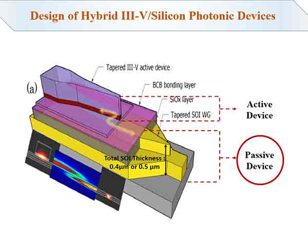
InP-based active layers on top of silica
Using InP-based active layers on top of silicon for photonic applications offers promise for high-performance, integrated components. Monolithic integration using InP-based compound semiconductors has a promising performance record, and manufacturing costs are attractive.
InP-based materials are known to have high mode confinement. This feature is important for compact devices. InP-based materials also exhibit band-filling effects. These effects allow the propagation of light through silicon devices governed by a variety of nonlinear optical phenomena. Nonlinear optical phenomena include two-photon absorption, the Kerr effect, and the Raman effect.
One promising application of InP-based active layers on top of silica is in the construction of high-efficiency phase shifters. InP-based materials also have stronger carrier-plasma effects than silicon. These effects permit the generation of all-optical signal routing.
Another InP-based application is the integration of a laser diode and a phase shifter. A typical vertical diode requires a silicon waveguide layer between 400 and 500 nm. InP-based layers on top of silicon waveguides are thin enough to enable a successful integration of a laser diode into a silicon waveguide circuit. However, this method is complicated and would increase fabrication costs.
The semiconductor industry has made many advances in processing and packaging. However, these improvements are not yet being used to benefit the photonics industry. Until now, the photonics industry has remained a foster child of the capital equipment industry.
New devices are required to meet the growing demands of all-optical networks without electrical regeneration. There are new devices in the works including all-optic switches, optical time-division multiplexers (OTDM), and wavelength converters based on the nonlinear effects in SOAs. New devices are also needed for instantaneous fault recovery and traffic reconfiguration.
Excitation of SAWs through the absorption of short pump pulses in structured metallic patterns
Traditionally, SAW-based RF signal processing was implemented through the absorption of short pump pulses in two-dimensional metal structures. This approach has been used in various RF applications, such as RF signal processing, filtering, and acousto-optic properties of materials. However, it could not compete with the strength of piezo-electric actuation of SAWs.
In this study, a more efficient method of excitation of SAWs was investigated. Photo-thermal excitation of SAWs has been shown to be a viable approach to sensing applications. However, photo-thermal excitation is not suitable for SAWs in the range of frequencies where piezo-electric actuation is sufficient. Instead, a continuous pump light scheme was introduced to provide better coupling to surface waves. This concept is scalable to higher frequencies. In addition, it may fulfill the requirements of microwave-photonic signal processing applications.
In this study, the excitation of SAWs is achieved by using structured metallic patterns. These patterns are designed to be periodic and accompanied by periodic contraction and expansion of the metals. In this way, SAWs are focused to a small spot.
The intensity of the pump light is modulated by a sine wave of a radio-frequency of interest. It is found that the absorption of this modulated pump light leads to periodic temperature changes in the metallic stripes. This can be used to increase the magnitude of the SAW. In addition, this method is scalable to shorter spatial periods. The SAW frequency can be reached up to 8 GHz at a L of 500 nm.
A standard SOI can be used for the fabrication of these photonic devices. These devices are functionally equivalent to traditional SAW-electronic devices. They can be used as integrated microwave-photonic filters with tens of megahertz wide passbands. However, the output SNR over the 20 MHz bandwidth is not suitable for many signal processing applications.
Microprocessor compatibility
Integrated optical devices fabricated using silicon on insulator (SOI) technology have a number of advantages, including enhanced processing capabilities and lower cost. But, because these devices require thin silicon films, they have limited volume for large-scale VLSI applications. A more practical material platform for high-performance optical signal processors is a silicon nitride waveguide.
Silicon nitride is a low-loss material, which makes it an ideal material for photonic RF filters with MHz-band frequency selectivity. In addition to its low loss characteristics, it also features high index-contrast, which is important for optical signal processing. In fact, it is the basis for a new silicon process technology developed by ST.
A number of advantages are associated with this technology, including improved performance, improved power management, and reduced cost. This technology is also suitable for military electronics applications, as it enables improved tolerance to transient radiation. But, for large-scale commercial applications, this technology is still at a developmental stage.
Another benefit of this technology is the fact that it is capable of implementing multiple functions in a single chip. This could reduce the unit cost of such chips, and could also pave the way for programmable photonic processors.
Other advantages of the technology include the fact that it offers a unique device structure, which could be advantageous for high-performance optical signal processors. This is in part due to the fact that it allows for higher packing density than bulk silicon. But, more importantly, the silicon on insulator (SOI) device structure offers reduced cost, improved performance, and greater yield. It also allows for the construction of isolated-substrate CMOS devices.
Integrated optical devices fabricated using SOI technology have been shown to be useful in many applications, including lasers, optical multiplexers, amplifiers, and detectors. However, these devices also have limitations, such as the need for separate optical carrier phase change to switch between bandpass filters and bandstop filters.