
One of the items in your “infrared materials” menu is “silicon, transmitting grade”.
However when I click, no wafers
are listed. Does this mean
they are not in stock? What
is the typical resistivity and
thickness for the transmitting
grade?
Silicon Wafer Refractive Index
A material's scientist requested a quote for the following:
UniversityWafer, Inc. Answered:
In the IR range from 1.5µm to 5.5µm, pure Silicon is perfectly transparent, meaning that its absorption is nil. In that range Silicon's transmittance in air is about 52% but that is because of its high refractive index. n-type Silicon with Ro>10 Ohmcm or p-type Silicon with Ro>20 Ohmcm is pure enough that its absorption is negligible.
Therefor, for a window in the 1.5-5.5µm range, any double-side-polished wafer that is n-type Ro>10 Ohmcm or p-type Ro>20 Ohmcm is suitable. For higher wavelengths, especially about 9.0µm FZ silicon might be recommended.
For 1.5-5.5µm range, for the list of wafers reference # 221700 for specs and pricing.
Get Your Quote FAST! Or, Buy Online and Start Researching Today!
Hi Res Float Zone Silicon Wafer Refractive Index
A PhD student requested the followng quote:
We need 2~3 pics of 2-mm thick, HiResist Float Zone Si Wafer: Diameter: 76.2mm or 50mm or any Dopant: No, highly pure Resistivity: >20,000 ohm-cm Thickness: 2 mm Surface finish: front, back both sides polished. Can you help to quote and then we can make an order immediately?
Question:
Oientation does not matter, Can you just double confirm the refractive index of this wafer?
Answer:
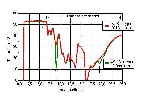
In the attachment is the IR Transmission Spectrum of Silicon. Red plot is that of FZ 50,000 Ohmcm material and Green plot is that of CZ 10 Ohmcmmaterial. There is no difference between 10 Ohmcm and 50,000 Ohmcm material, but there is a difference between FZ and CZ material. The reason is that CZ contains about 20ppma of dissolved Oxygen and about 1 ppma of Carbon whereas FZ contains <0.5ppma of Oxygen and <0.5ppma of Carbon. This shows up as Carbon and Oxygen absorption bands at 6.0µm, 9.0µm and 19.0µm. CZ material absorbs more and so its transmittance is lower at these wavelengths.
You will notice that even in the most transparent region (1.5 to 5.5)µm Transmittance is barely over 50 %. This is because of reflections from both sides of the wafer. These reflections are very strong because of the very high refractive index of Silicon in comparison to that of air. This can only be mitigated by "Anti-Reflection Coatings.
tem Qty. Description
FN94. 3/10/25 Silicon wafers, per SEMI Prime, P/P 3"Ø×2,000±25µm, FZ Intrinsic undoped Si:-[111]±0.5°, Ro > 20,000 Ohmcm, Both-sides-polished, SEMI Flat (one), Sealed in Individual Wafer cassette.
Reference #235699 for specs and pricing.
What is the Refractive Index of Substrates?
The refractive index (n) of a medium is a dimensionless number that describes how light, or any other radiation, propagates through that medium. It's defined as the speed of light in vacuum divided by the speed of light in the medium.
The refractive index can vary for different substances, and even within the same substance it can change depending on the wavelength of light and the temperature.
Here are refractive indices for some common materials at room temperature:
- Vacuum: 1 (by definition)
- Air: approximately 1.0003
- Water: approximately 1.33
- Glass: typically around 1.5, but it varies depending on the type of glass
- Diamond: approximately 2.42
However, when you mention "substrates", it's a bit ambiguous. A substrate can be any material upon which another material is deposited or applied. So, the refractive index of a substrate could range widely depending on the actual material used. For a specific refractive index, you would need to know the specific material of the substrate.
- Silicon (Si): about 3.42
- Gallium Arsenide (GaAs): about 3.3 - 3.5
- Indium Phosphide (InP): about 3.1 - 3.5
- Silicon Carbide (SiC): about 2.65
- Sapphire (Al2O3): about 1.76
- Glass: typically around 1.5, but it varies depending on the type of glass
Please note these values can vary depending on the wavelength of light and the temperature, among other factors. For precise refractive index values for your specific application, it's best to refer to the manufacturer's data or perform a specific measurement.
If you need specific refractive indices for any other substrate material, feel free to ask!
Substrates Used for Neutron Reflectometry Experiments
A postdoctoral researcher requested the following:
I am interested in attaining a silicon substrate that is identical to what is used for Neutron Reflectometry experiments, but around 100 micrometers thick so that I can use TIRF microscopy as an orthogonal technique to study the same system we take NR data on. Is a 100 micrometer thick Silicon wafer transparent enough to be used for Total Internal Reflection Fluoresence Microscopy?
For Neutron Reflectometry we normally offer wafers that are either p-type Boron doped Silicon of crystallographic orientation (100) {Si:B[100]} or n-type Phosphorus doped Silicon {Si:P[100]} at purity level corresponding to Ro>1 Ohmcm. The important characteristic is that such wafers be flats, that is with Total Thickness Variation (TTV) <10µm. Normally, such wafers are thick, often 3mm thick, and one-side-polished.
You certainly need Double-Side-Polished wafers for otherwise, the unpolished side will diffuse whatever radiation you use in your microscopy. Wafers 100µm thick are very thin and therefore expensive, especially in larger diameters. In the visible range (0.3 to 1.0)µm Silicon is opaque. In the near IR range (1.2-5.0)µm, Silicon, both CZ and FZ, has very low absorption, for all resistivities > p-type 20 Ohmcm or > n-type 10 Ohmcm {of course Silicon has a high Refractive Index so transmission in air is limiter to about 50%}. In the IR range (5-10)µm in which Silicon exhibits absorption bands due to Oxygen and to Carbon, FZ crystallized Silicon is better than the more commonly used CZ crystallized Silicon.
P/P 2"Ø×100±15µm FZ n-type FZ Si:P[100], Ro>10 Ohmcm, TTV<10µm.
Reference #205311 for specs and pricing.
Zinc Oxide (ZnO) Witness Refractive Index
A PhD candidate requested the following quote:
Do you have 1’’ polished ZnO in stock? We are looking for ZnO witness with the refractive index of 1.94 at 1.0 um wavelength.
Yes we have 1'' polished ZnO with the refractive index of 1.94 at 1.0 um wavelength. But we still need to know the thickness and polish requirement and quantity. So that we could quote you a more exact price.
Reference #221531 for specs and pricing.
Quartz Substrates for Terahertz Spectroscopy and Terahertz Photonic Technology
A Leader of TeraHertz Biophotonics requested the following quote:
We got our well packed sample and everything looks perfect.
We will use the material for Terahertz spectroscopy and Terahertz photonic technology since Quartz has the good habit to be transparent
both in the terahertz and visible and relativly low refractive index in
the teraherz (n=2) .
Reference #54873 for specs and pricing.