Substrates used to Fabricate Nanostructures
UniversityWafer supplies research-grade substrates for nanostructure fabrication, including silicon, silicon-on-insulator (SOI), sapphire, fused silica, quartz, silicon nitride, and thermal oxide wafers. Our materials support advanced research in electron beam lithography (EBL), MEMS, photonics, plasmonics, quantum devices, nanosensors, and semiconductor nanotechnology, with custom specifications available for both prototype and production applications.
Request a Quote for Nanostructure Research Substrates
UniversityWafer supplies research-grade substrates for nanostructure fabrication, including silicon, silicon-on-insulator (SOI), fused silica, quartz, thermal oxide, sapphire, silicon nitride, and specialty coated wafers. Our materials are used by universities, government laboratories, and commercial R&D groups developing MEMS, photonics, plasmonics, quantum devices, and nanoscale electronics.
One university researcher requested substrates for fabricating silicon nanostructures using electron beam lithography:
Research Inquiry:
 "We are fabricating silicon nanostructures with silicon film thicknesses between 300 nm and 700 nm. The substrate should be SiO2 or another transparent insulator, and we plan to use SOI wafers for electron beam lithography. Do you offer silicon films within this thickness range?"
Reference #205719 for specifications and pricing.
Another researcher requested p-GaN / n-ZnO heterojunction substrates for light-emitting devices based on semiconductor nanostructures.
"I will use p-GaN / n-ZnO nanostructure heterojunctions for a light-emitting diode. Please provide a quotation."
Reference #38046 for specifications and pricing.
Get Your Quote FAST! Or, Buy Online and Start Researching Today!
Popular Nanostructure Research Materials
- Silicon wafers
- Silicon-on-Insulator (SOI) wafers
- Thermal oxide coated silicon
- Silicon nitride coated wafers
- Fused silica and quartz wafers
- Sapphire substrates
- Gallium nitride (GaN)
- Silicon carbide (SiC)
Need a custom substrate? Include your material, film thickness, orientation, surface finish, and quantity in the form above, and our engineering team will recommend the best substrate for your nanotechnology research.
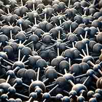
What Are Nanostructures?
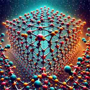 Nanostructures are materials or devices with at least one dimension between 1 and 100 nanometers. At this scale, materials often exhibit unique electrical, optical, magnetic, thermal, and mechanical properties that differ significantly from their bulk counterparts. These characteristics make nanostructures essential for next-generation electronics, photonics, energy devices, biomedical engineering, and quantum technologies.
Researchers fabricate nanostructures using advanced techniques such as physical vapor deposition (PVD), chemical vapor deposition (CVD), electron beam lithography (EBL), photolithography, sputtering, reactive ion etching (RIE), and atomic layer deposition (ALD).
Common Types of Nanostructures
- Nanoparticles – Used in catalysis, drug delivery, imaging, and sensors.
- Nanowires – Applied in transistors, LEDs, batteries, and nanosensors.
- Carbon Nanotubes (CNTs) – High-strength conductive materials for electronics and composites.
- Nanoporous Materials – Used in filtration, catalysis, and energy storage.
- Nanocomposites – Improve mechanical, electrical, and thermal properties.
- Nanolaminates – Engineered multilayer films for optics and protective coatings.
- Nanofibers – Common in biomedical devices, filtration, and flexible electronics.
- Quantum Structures – Quantum dots and related materials for photonics and quantum computing.
Best Substrates for Nanostructure Fabrication
The substrate plays a critical role in nanostructure performance by affecting crystal quality, thermal conductivity, optical transmission, electrical behavior, and fabrication compatibility. The most common research substrates include:
Applications of Nanostructures
Nanostructures are enabling breakthroughs across numerous industries. Current research includes:
- Semiconductor device fabrication
- Integrated photonics
- MEMS and NEMS devices
- Quantum computing
- Plasmonic sensors
- Metasurfaces and flat optics
- Solar cells and energy harvesting
- Biomedical diagnostics
- Spintronic devices
- Optoelectronic components
Research-Grade Substrates for Nanotechnology
UniversityWafer supplies high-quality silicon, SOI, sapphire, fused silica, quartz, silicon nitride, thermal oxide, silicon carbide, gallium arsenide, graphene, and other specialty substrates for nanotechnology research. Our materials are used by universities, government laboratories, and commercial R&D groups developing next-generation electronic, optical, and quantum devices.
Related Nanotechnology Resources
