
Metalloid Elements in Semiconductor Research
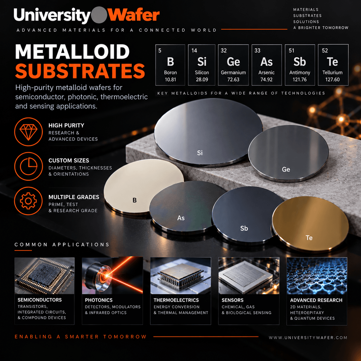
Metalloids are elements that display a combination of metallic and nonmetallic properties. Their controllable electrical conductivity, covalent bonding, and compatibility with semiconductor fabrication make several metalloid elements important in electronics, photonics, sensors, solar cells, and advanced materials research.
The classification of some elements can vary, but the most commonly recognized metalloids used in semiconductor technology include boron, silicon, germanium, arsenic, antimony, and tellurium.
Common Metalloid Elements and Their Uses
- Boron (B) – Commonly introduced into silicon wafers as a p-type dopant. Boron doping increases the concentration of holes available for electrical conduction.
- Silicon (Si) – The most widely used semiconductor material and the foundation of integrated circuits, MEMS, sensors, solar cells, and power devices.
- Germanium (Ge) – Used in infrared optics, photodetectors, high-speed electronics, silicon-germanium devices, and multi-junction solar cells.
- Arsenic (As) – Used as an n-type dopant in silicon and as a component of compound semiconductors such as gallium arsenide.
- Antimony (Sb) – Used as an n-type dopant in silicon and germanium for specialized semiconductor devices.
- Tellurium (Te) – Used in infrared detectors, thermoelectric materials, photovoltaic devices, and compound-semiconductor research.
Why Are Metalloids Important?
Most metalloids are positioned near the stair-step boundary separating metals and nonmetals on the periodic table. Their electrical conductivity generally falls between that of conductive metals and insulating nonmetals.
In semiconductor fabrication, conductivity can be modified by adding controlled amounts of dopant atoms. For example, boron can create p-type silicon, while arsenic, phosphorus, or antimony can produce n-type silicon. This ability to control charge carriers is essential for fabricating transistors, diodes, integrated circuits, sensors, and photovoltaic devices.
Semiconductor Materials Available
UniversityWafer supplies research and production substrates including silicon wafers, germanium wafers, SOI wafers, silicon carbide wafers, and gallium arsenide wafers.
To request a quote, provide the material, diameter, thickness, crystal orientation, dopant, resistivity, surface finish, and quantity needed. Our team can also help identify a suitable substrate when your final specifications are still being developed.
Get Your Semiconductor Wafer Quote FAST! Complete the form below or Buy Online and start researching today.
What Makes an Element a Metalloid?
Metalloids are elements that exhibit properties between those of metals and nonmetals. They may have a metallic appearance, but they are often brittle and conduct electricity less efficiently than true metals. Their intermediate electrical behavior makes several metalloid elements especially important in semiconductor materials, electronics, photonics, solar cells, and advanced research.
Commonly recognized metalloids include boron, silicon, germanium, arsenic, antimony, and tellurium. Among these, silicon and germanium are especially valuable because their electrical conductivity can be controlled for semiconductor device fabrication.
Is Germanium a Metal, Nonmetal, or Metalloid?
 Germanium (Ge) is classified as a metalloid. It combines characteristics of both metals and nonmetals, including a metallic-looking surface, brittle mechanical behavior, covalent bonding, and controllable electrical conductivity.
Germanium is located in Group 14 of the periodic table with carbon, silicon, tin, and lead. Like silicon, germanium has four valence electrons and forms a diamond-cubic crystal structure. These properties allow germanium to function as a semiconductor in electronic and optoelectronic devices.
Why Is Germanium Considered a Metalloid?
- Semiconductor behavior: Pure germanium conducts electricity better than most nonmetals but less efficiently than metals. Its conductivity can be adjusted through doping.
- Metallic appearance: Germanium has a gray-white metallic luster even though it does not behave mechanically like a typical metal.
- Brittle structure: Unlike malleable metals, germanium is brittle and can fracture when mechanically stressed.
- Covalent bonding: Germanium commonly forms covalent bonds, a characteristic associated with nonmetallic elements.
- Intermediate electrical properties: Germanium's electrical behavior lies between that of conductive metals and insulating nonmetals.
Germanium Atomic Structure
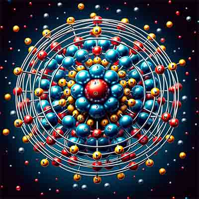
Germanium has an atomic number of 32. A neutral germanium atom therefore contains 32 protons and 32 electrons. The number of neutrons varies by isotope.
Its electrons are arranged in shells as follows:
- First shell: 2 electrons
- Second shell: 8 electrons
- Third shell: 18 electrons
- Fourth shell: 4 valence electrons
The four electrons in germanium's outer shell explain why it behaves similarly to silicon. These valence electrons participate in covalent bonding and help form the crystal lattice used in semiconductor wafers and electronic devices.
Germanium in Semiconductor Research
Germanium wafers are used in applications that benefit from high carrier mobility, infrared transparency, and compatibility with compound-semiconductor and silicon-germanium technologies.
Common germanium wafer applications include:
- Infrared optics and thermal imaging
- Photodiodes and photodetectors
- High-speed transistors and RF electronics
- Gamma-ray and X-ray detectors
- Multi-junction solar cells
- Silicon-germanium device research
- Epitaxial growth and thin-film deposition
- Advanced electronic and optoelectronic devices
Germanium Compared with Silicon
Germanium and silicon are both Group 14 metalloids used as semiconductor materials. However, each offers different advantages. Silicon wafers remain the most widely used substrates because they are commercially available, thermally stable, and capable of forming high-quality silicon dioxide insulating layers.
Germanium offers higher electron and hole mobility than silicon, making it attractive for high-speed devices. It is also transparent across important infrared wavelengths, which makes germanium useful for infrared optics, detectors, and photonic systems.
Common Metalloids in Semiconductor Technology
- Boron (B): Commonly used as a p-type dopant in silicon wafers.
- Silicon (Si): Used for integrated circuits, MEMS, sensors, solar cells, and most conventional semiconductor devices.
- Germanium (Ge): Used for infrared optics, photodetectors, high-speed electronics, and SiGe devices.
- Arsenic (As): Used as an n-type dopant and as a component of gallium arsenide.
- Antimony (Sb): Used as an n-type dopant in silicon and germanium.
- Tellurium (Te): Used in thermoelectric, infrared detector, and photovoltaic materials.
Choosing Germanium Wafers
When ordering germanium substrates, researchers may need to specify the wafer diameter, crystal orientation, thickness, conductivity type, dopant, resistivity, surface finish, edge profile, and quantity. Germanium wafers may also be selected for electrical-grade, optical-grade, epitaxial, or detector applications.
UniversityWafer supplies germanium wafers, silicon wafers, SOI wafers, silicon carbide wafers, and other semiconductor substrates for research, device development, and production.