Helping Process Integration Engineers Source Semiconductor Wafers
UniversityWafer supports Process Integration Engineers with high-quality semiconductor wafers, sapphire substrates, GaN epi-wafers, glass wafers, and highly doped silicon for semiconductor fabrication, MEMS processing, photonics, and micro nano fabrication research.
Our wafer inventory includes silicon, sapphire, SOI, GaN, quartz, glass, and thin film coated substrates available in multiple diameters, orientations, thicknesses, and resistivity ranges for advanced semiconductor applications.
Sapphire Wafer Specifications for Semiconductor Research
A Process Integration Engineer requested assistance sourcing custom sapphire wafers for semiconductor and microfabrication research applications.
We are looking for C-plane sapphire wafers <0001> +/- 1 degree or 45 degree CCW C-axis projection onto the R-plane +/- 1 degree.
Desired wafer diameters include 100 mm, 150 mm, and 200 mm with thicknesses ranging from 0.7 mm to 2 mm. Double-side polished (DSP) sapphire wafers with scratch/dig 60/40 specifications are preferred.
Additional interest was expressed in similar diameter and thickness options for silicon substrates compatible with semiconductor process integration and SEMI manufacturing standards.
Reference #259392 for specifications, availability, and pricing.
Highly Doped Silicon Wafers for MEMS and Micro Nano Fabrication
A university micro nano fabrication department requested P++ silicon wafers for semiconductor device fabrication and MEMS research.
Requested specifications included highly doped silicon wafers with 0.0008 ohm-cm resistivity and 100-200 nm LPCVD silicon nitride coatings.
The request also included the possibility of a thin SiO2 thermal oxide layer beneath the nitride film for semiconductor processing applications.
Reference #196764 for specifications and quantity requirements.
Need Semiconductor Wafers FAST?
Buy Online Today or request a custom quote for your semiconductor process integration project.
Glass Wafer Thermal Expansion Requirements
Process Integration Engineers often require glass wafers with specific thermal expansion coefficients for semiconductor packaging, MEMS devices, photonics, and microfabrication applications.
A customer requested glass wafers with coefficients of thermal expansion (CTE) between 2 and 6 ppm/°C for advanced semiconductor and thin film processing applications.
Reference #246369 for specifications and pricing.
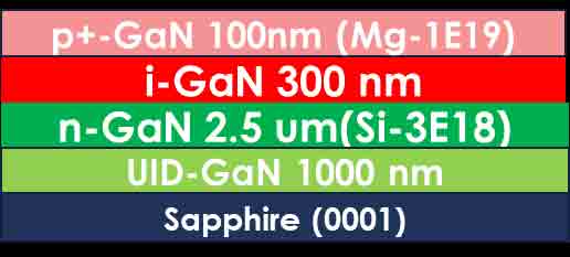
GaN Epi-Structure Wafers for Semiconductor Devices
A principal Process Integration Engineer requested a quotation for custom GaN on sapphire epi-structure wafers used in semiconductor device development.
Requested structure:
- p+-GaN 100 nm (Mg-1E19)
- i-GaN 2.5 µm (Si-3E18)
- UID-GaN 1000 nm
- Sapphire (0001)
Wafer size requested: 50 mm (2-inch)
Quantity requested: 25 wafers
Additional requirements included:
- Surface roughness < 0.5 nm
- FWHM < 300 arc sec
- XRD characterization
- AFM surface analysis
- Hall measurements for p-GaN and n-GaN layers
The customer also requested estimated p-GaN mobility values to assist with optimization of p-GaN ohmic contacts in semiconductor device processing.
Reference #268720 for specifications and quantities.
Skills Needed for Process Integration Engineering
Process Integration Engineers working in semiconductor manufacturing and MEMS fabrication typically require experience with cleanroom processing, wafer bonding, semiconductor process development, and advanced wafer characterization techniques.
MEMS Process Integration Engineers often work with DRIE processing, wafer bonding modules, failure analysis (FA), yield improvement, and next-generation electrostatic actuator technologies.
- Strong understanding of silicon processing, vacuum science, and semiconductor manufacturing.
- Hands-on experience with cleanroom fabrication, RIE etching, wafer bonding, and thin film processing.
- Experience with MEMS devices, semiconductor process simulation, and electrostatic actuator technologies.
- Strong troubleshooting, communication, and semiconductor project management skills.
What Does a Process Integration Engineer Do?
Process Integration Engineers play a critical role in semiconductor manufacturing by developing, optimizing, and integrating wafer fabrication processes used to produce advanced electronic devices. These engineers help ensure that silicon wafers, MEMS devices, thin films, and semiconductor substrates meet strict performance, reliability, and yield requirements throughout production.
Process integration combines multiple fabrication steps including deposition, photolithography, etching, wafer bonding, oxidation, and inspection into a streamlined semiconductor manufacturing workflow. Process Integration Engineers work closely with cleanroom teams, R&D scientists, and manufacturing specialists to improve device performance and production efficiency.
-
Process Development and Optimization
- Develop and optimize semiconductor fabrication processes for advanced device manufacturing.
- Improve wafer yield, device reliability, and manufacturing efficiency.
- Refine thin film deposition, photolithography, oxidation, and etching techniques.
- Support process scaling for research, prototyping, and high-volume semiconductor production.
-
Cross-Functional Collaboration
- Collaborate with design engineers, cleanroom operators, quality assurance teams, and manufacturing specialists.
- Ensure compatibility between materials, wafer processes, and semiconductor device architectures.
- Support technology transfer from research and development into production environments.
-
Troubleshooting and Yield Improvement
- Identify and resolve semiconductor process integration issues affecting wafer yield and device performance.
- Perform root cause analysis on contamination, defects, film stress, and process variability.
- Optimize process conditions for MEMS fabrication, microelectronics, and advanced semiconductor devices.
-
Data Analysis and Process Monitoring
- Collect and analyze process data from multiple fabrication stages.
- Use statistical process control (SPC) methods to monitor semiconductor manufacturing stability.
- Track wafer thickness, film uniformity, defect density, and electrical performance metrics.
-
Thin Film Deposition and Wafer Processing
- Work with technologies such as LPCVD, PECVD, ALD, thermal oxidation, and epitaxy.
- Support processing of silicon substrates, sapphire wafers, SOI wafers, and GaN substrates.
- Develop processes for dielectric films, nitride coatings, and semiconductor device layers.
-
Process Documentation and Quality Assurance
- Create detailed process flows, work instructions, and manufacturing documentation.
- Maintain semiconductor quality standards and support cleanroom compliance procedures.
- Assist with process audits, validation testing, and manufacturing traceability.
-
Advanced Semiconductor Technologies
- Stay current with emerging semiconductor manufacturing technologies and wafer processing techniques.
- Support research involving GaN on sapphire, silicon carbide, photonics, and advanced MEMS devices.
- Evaluate new materials, substrates, and process architectures for next-generation semiconductor applications.
Common Materials Used by Process Integration Engineers
Process Integration Engineers frequently work with a wide range of semiconductor substrates and thin film materials depending on device requirements and fabrication goals. Common materials include silicon wafers, SOI wafers, sapphire substrates, glass wafers, gallium nitride (GaN), silicon carbide (SiC), quartz, and thermal oxide coated wafers.
These materials are widely used in semiconductor manufacturing, MEMS fabrication, photonics, RF devices, power electronics, sensors, and advanced research applications requiring high-performance wafer processing and integration.
Need Semiconductor Wafers FAST?
Buy Online Today or request a custom quote for your process integration engineering project.
