Custom Silicon Wafer Dicing Services
UniversityWafer provides custom silicon wafer dicing services
for researchers, engineers, universities, laboratories, and semiconductor
companies that need full wafers converted into smaller dies, chips, squares,
rectangles, or coupons.
Dicing projects can be specified by wafer diameter, thickness, crystal
orientation, resistivity, surface finish, die dimensions, dimensional
tolerance, quantity, and packaging requirements. Starting substrates may
include intrinsic or doped silicon, high-resistivity material, oxide-coated
wafers, and
double-side polished silicon wafers
.
Depending on the project requirements, finished pieces may also require
tape mounting, individual handling, protective packaging, or wafer-cassette
storage. Providing the intended application and complete specifications
helps determine the appropriate dicing and handling approach.
Custom Diced Silicon for Spectroscopy Research
One university Ph.D. researcher requested high-resistivity
diced silicon wafers for spectroscopy research. The project
required small silicon dies with tightly defined material specifications.
The researcher requested
undoped silicon wafers
diced into 10 mm × 10 mm pieces.
- Die dimensions: 10 mm × 10 mm
- Wafer thickness: 525 µm
- Surface finish: Single-side polished
- Crystal orientation: <100>
- Material: Undoped silicon
- Resistivity: Greater than 10,000 ohm-cm
- Quantity: 20 pieces
The finished silicon dies were intended for
positron annihilation spectroscopy
.
Reference inquiry #270386 for example specifications and pricing.
Request a Custom Silicon Wafer Dicing Quote
For the most accurate quote, include the starting wafer material,
wafer diameter and thickness, requested die dimensions, dimensional
tolerance, surface finish, resistivity, crystal orientation, quantity,
and any special cleaning or packaging requirements.
Get Your Silicon Wafer Dicing Quote FAST!
Or
Buy Online
and Start Researching Today!
Silicon Wafer Dicing, Handling and Packaging
Dicing is only one part of preparing silicon dies for research.
Surface cleanliness, handling, storage, and packaging can also be
important when the starting material has demanding electrical or
surface specifications.
A senior research and development physicist contacted UniversityWafer
about dicing and packaging
RCA-cleaned silicon wafers
while reducing the risk of contamination during storage and shipment.
Example custom dicing specification:
Item IS92b — Quantity: 4 wafers
-
Material: Float-zone intrinsic
undoped silicon
- Wafer diameter: 4 inches, 100.0 ± 0.5 mm
- Starting wafer thickness: 3,000 ± 25 µm
- Requested die dimensions: 21 mm × 21 mm
- Side-length tolerance: ±0.2 mm
- Crystal orientation: <100> ± 0.5°
- Resistivity: Greater than 20,000 ohm-cm
- Minority-carrier lifetime: Greater than 1,000 µs
-
Surface finish:
both sides polished
- Surface roughness: Ra less than 1 nm, process guarantee
- Edge configuration: One flat
- Estimated yield: Approximately six squares per wafer
-
Packaging specification: Pieces mounted on blue tape and placed
in individual protective wafer cassettes
This example demonstrates how a wafer dicing project may involve more
than die dimensions alone. Electrical properties, crystal orientation,
surface roughness, polishing, dimensional tolerance, handling, and
packaging may all be important to the final application.
Reference inquiry #23278 for example specifications and pricing.
Silicon Wafer Dicing Services
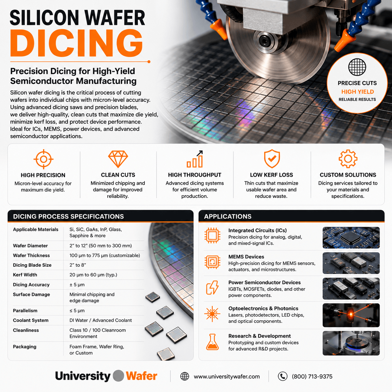
Silicon wafer dicing is the process of cutting a full
silicon wafer
into smaller dies, chips, squares, rectangles, or coupons.
UniversityWafer works with researchers, engineers, laboratories, and
semiconductor companies that require custom diced substrates for device
fabrication, testing, thin-film deposition, MEMS, photonics, sensors,
spectroscopy, and materials research.
Dicing requirements can vary significantly depending on wafer diameter,
thickness, crystal orientation, surface finish, coatings, resistivity,
requested die size, tolerance, and final application. Providing complete
specifications helps determine the most appropriate cutting and handling
approach.
How Does Silicon Wafer Dicing Work?
Wafer dicing, also called wafer singulation, separates a
wafer into individual pieces after crystal growth, polishing, coating,
lithography, deposition, or other processing steps. The cutting approach
depends on the material and the condition of the wafer before dicing.
Important considerations include die dimensions, kerf width, edge quality,
wafer thickness, surface coatings, patterned device areas, particle control,
mechanical stress, and the risk of chipping or cracking.
Mechanical Blade Dicing
Mechanical blade dicing uses a precision spindle and thin
diamond-embedded blade to cut along predefined dicing streets.
It is widely used for silicon because it can provide repeatable cuts
and controlled die dimensions across many standard wafer thicknesses.
Blade selection, spindle speed, feed rate, coolant flow, wafer mounting,
and cut depth all influence edge quality and dimensional accuracy.
Mechanical dicing is commonly considered for silicon coupons, sensor
substrates, test pieces, rectangular dies, and research samples.
Laser Wafer Dicing
Depending on project requirements and available processing options,
laser-based dicing may be considered for specialized applications.
Laser wafer dicing uses focused laser energy to create
a separation path through or within the substrate. Because there is no
physical saw blade in contact with the wafer, laser-based processes may
be useful for thin substrates, narrow cutting streets, fragile structures,
or applications requiring specialized geometries.
Wavelength, pulse duration, laser power, scanning speed, wafer thickness,
coatings, metallization, and dielectric layers can affect kerf width,
heat input, debris generation, and final edge quality.
Other Wafer Singulation Methods
Other wafer singulation techniques used in the semiconductor industry
include scribe-and-break processing, stealth dicing, thermal laser
separation, and plasma dicing. The suitability of each method depends
on wafer material, thickness, device geometry, required edge quality,
allowable thermal exposure, and contamination requirements.
These methods are generally selected for specialized applications where
narrow separation paths, reduced mechanical contact, low particle
generation, or non-standard die geometries are important.
Materials and Wafer Types for Dicing
Custom dicing may be required for many types of silicon substrates,
including:
Custom Die Sizes and Dicing Tolerances
Custom diced silicon can be supplied as squares, rectangles, dies,
chips, or coupons. Final dimensions and tolerances depend on the starting
wafer, thickness, cutting method, surface condition, and application.
When requesting a quote, specify the desired finished die dimensions and
any important requirements for dimensional tolerance, edge condition,
kerf width, orientation, or usable surface area.
How to Specify a Silicon Wafer Dicing Job
To receive an accurate quote for silicon wafer dicing services,
provide as many of the following details as possible:
- Wafer material
- Wafer diameter
- Wafer thickness and thickness tolerance
- Requested die length and width
- Dimensional tolerance
- Crystal orientation, such as <100> or <111>
- Conductivity type and dopant
- Resistivity range
- Single-side or double-side polished surface
- Oxide, nitride, metal, or other surface coatings
- Patterned structures or device features
- Cleaning requirements
- Tape mounting or individual die handling
- Packaging requirements
- Quantity of wafers or finished dies
Cleaning and Packaging After Dicing
Post-dicing handling can be especially important for polished,
high-resistivity, coated, or device-grade silicon. Depending on the
project, requirements may include tape mounting, individual die handling,
wafer-cassette packaging, protective containers, or controlled cleaning.
For projects requiring cleaner silicon surfaces, review our
RCA wafer cleaning services
.
Packaging and handling requirements should be specified when requesting
a quote so the finished pieces can be prepared appropriately.
Applications for Diced Silicon Wafers
Custom diced silicon dies and coupons are used across semiconductor,
engineering, and research applications, including:
- MEMS fabrication
- Semiconductor device development
- Microelectronic packaging
- Thin-film deposition
- Photolithography and process development
- Optical and photonic research
- Sensor development
- Spectroscopy and surface analysis
- Materials characterization
- Prototype fabrication
- University laboratory research
Diced Silicon Wafers vs. Wafer Dicing Services
Customers looking for a finished silicon piece may also want to review our
diced silicon wafers
page. This wafer dicing page focuses primarily on the
cutting and singulation service, while the diced silicon
wafer page focuses on finished silicon dies, chips, and coupons supplied
to customer specifications.
Request a Silicon Wafer Dicing Quote
UniversityWafer can help with custom silicon wafer dicing requirements
for research, prototyping, device development, testing, and semiconductor
processing. Send us your wafer specifications, requested die dimensions,
tolerances, quantity, and packaging requirements so we can review the
project.
Related Silicon Wafer Dicing Resources
-
Diced Silicon Wafers
– Explore finished silicon dies, chips, squares, rectangles, and coupons prepared to custom dimensions.
-
Silicon Wafers
– Browse silicon wafer grades, diameters, orientations, resistivities, dopants, thicknesses, and surface finishes.
-
Wafer Processing Services
– Learn about additional wafer processing options for research, prototyping, and semiconductor development.
-
Double-Side Polished Silicon Wafers
– Find silicon substrates with polished front and back surfaces for precision research and device applications.
-
Undoped Silicon Wafers
– Explore intrinsic and high-resistivity silicon for spectroscopy, sensors, electronics, and materials research.
-
RCA Wafer Cleaning
– Learn about silicon wafer cleaning options before dicing, coating, fabrication, or packaging.
-
Thermal Oxide Silicon Wafers
– Explore silicon wafers with thermal SiO₂ layers that may also require custom dicing into smaller dies.
-
Silicon-on-Insulator (SOI) Wafers
– Learn about SOI substrates used in MEMS, sensors, photonics, and advanced semiconductor devices.
-
Silicon Wafer Thickness Range
– Compare standard and custom wafer thicknesses that can affect dicing method, handling, and die strength.
-
Photolithography Process
– See how wafers are patterned before subsequent processing and die singulation.
