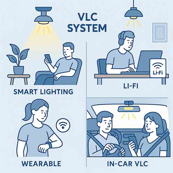
Thermal Oxide Wafers Used to Fabricate Visual Communication Devices (VLC)
A university lab manager requested a quote for the following.
Our lab work on Visual Comminucation Devices (VLC). I would like to know if you have available 4" SiO2 wafers doped with germanium with a thickness higher than 3 microns. ( the typical silica wafers employed in photonics PLCs)?
Can you provide together with the quote, data about the doping level and refractive index of the layers?
Reference #131213 for specs and quantity.
Get Your Quote FAST! Or, Buy Onlineand Start Researching Today!
What substrates are used to fabricate Visible-Light Communications Systems
Visible-Light Communication (VLC) systems, including Li-Fi and other optical wireless technologies, rely on optoelectronic devices like LEDs and photodetectors. The substrates used to fabricate these components must support efficient light emission and detection in the visible spectrum (400–700 nm). Here are the most common substrates used in VLC system fabrication:
🔷 1. Gallium Nitride (GaN)
-
Use: Blue, green, and white LEDs (main light source in VLC)
-
Why: Wide bandgap (~3.4 eV), high efficiency in visible-light emission
-
Substrates:
-
Sapphire (Al₂O₃): Most common for GaN epitaxy due to lattice compatibility and low cost
-
Silicon Carbide (SiC): Better thermal conductivity, used for high-power devices
-
Silicon (Si): Cost-effective, large wafer sizes, though with higher lattice mismatch
-
Bulk GaN: Ideal but expensive
🔷 2. Indium Phosphide (InP)
-
Use: Photodetectors and high-speed optoelectronics
-
Why: Direct bandgap, suitable for high-speed photodetectors and modulators
-
Substrates:
🔷 3. Gallium Arsenide (GaAs)
-
Use: Red and near-IR LEDs, photodetectors
-
Why: Efficient red-light emission, suitable for integrated optoelectronics
-
Substrates:
🔷 4. Silicon (Si)
-
Use: CMOS-based VLC transceivers, modulators, integrated circuits
-
Why: Low cost, mature fabrication technology
-
Note: Not efficient for light emission but widely used for photodiodes and electronics
🔷 5. Transparent Substrates
For display-integrated VLC:
-
Glass (e.g., borosilicate or fused silica): For transparent displays and optical waveguides
-
ITO-coated glass or polymer: For transparent electrodes in flexible VLC systems
🔷 6. Organic and Polymer Substrates
-
Use: Flexible and wearable VLC systems
-
Why: Lightweight, flexible, and printable
-
Example: PET (polyethylene terephthalate), PEN (polyethylene naphthalate)
Summary Table:
| Material |
Typical Use in VLC |
Advantages |
Substrate Type |
| GaN |
Visible LEDs |
High brightness, efficient in blue/green |
Sapphire, SiC, Si |
| GaAs |
Red LEDs, photodetectors |
Good optoelectronic properties |
GaAs |
| InP |
High-speed photodetectors |
High carrier mobility |
InP, GaAs, Si (with buffer) |
| Si |
Electronics, detectors |
CMOS-compatible, low cost |
Si |
| Glass/Quartz |
Transparent optical systems |
Transparent, stable |
Glass |
| Polymers |
Flexible VLC |
Printable, bendable |
PET, PEN |


