
Get Your Quote FAST! Or, Buy Online and Start Researching Today!
<Common specs researchers request
- P-type (Boron) and N-type (Arsenic/Antimony)
- Orientations: (100), (111), (110)
- Prime, test, and mechanical grades
- Polish options: SSP and DSP (when available)
Not sure what you need? Send your process notes and we’ll help narrow down the right wafer for your tool set.
Related pages
- Undoped Silicon Wafers
- Mechanical Grade Silicon Wafers
- SUMCO Wafers
- Silicon Carbide Wafers
- Silicon Wafer Suppliers
4, 6, and 8 Inch Wafers Explained: Choosing the Right Diameter for Research and U.S. Fabs
Choosing between 4", 6", and 8" silicon wafers is not just a diameter preference. It affects die count per wafer, tool compatibility, process control, cost per die, lead times, and long-term scalability. For U.S. labs and specialty fabs, the “best” wafer size is usually the one that matches your current equipment set and your roadmap for yield and volume.
Key takeaways
- 4 inch (100mm) is ideal for low-volume research, early prototypes, and legacy toolsets.
- 6 inch (150mm) is a practical “sweet spot” for MEMS, analog, and power devices in mature specialty lines.
- 8 inch (200mm) improves throughput and cost per die, and aligns with modernized 200mm tool ecosystems.
- Diameter sets throughput and equipment requirements, while grade and doping define performance and usability.
Quick answers: 4", 6", or 8"?
| Question | Short answer |
|---|---|
| When are 4" wafers best? | Low-volume research, early prototyping, teaching labs, and legacy equipment. Great for fast iteration and small lots. |
| Why do many fabs still use 6"? | 150mm supports profitable specialty devices with manageable capex and solid die count, especially for MEMS and power. |
| What makes 8" attractive? | Higher throughput and better cost per die compared with 100mm/150mm, with strong 200mm tool availability. |
| Does grade and doping matter as much as diameter? | Yes. Diameter affects throughput, but grade (prime/test/mechanical) and doping (P/N/undoped) drive electrical and surface requirements. |
1) Why wafer diameter matters
Wafer diameter affects how many dies you can print per wafer, how uniform your process can be across the surface, and which tools you can run. In practice, a larger diameter typically lowers cost per die when your equipment and process flow can support it. For many teams, the real limiter is not the wafer itself, but whether your lithography, deposition, etch, and metrology tools are designed for that size.
2) 4 inch (100mm) silicon wafers
Four-inch wafers are a workhorse for university labs, pilot lines, and legacy production. They are easy to handle, widely supported by older tools, and often available in small quantities with many common specifications.
Typical 4" specs you can source
- Doping: P-type (boron, gallium), N-type (arsenic, antimony), and undoped options.
- Orientation: (100), (111), (110) are common.
- Grades: Prime, test, and mechanical grade depending on your surface and defect needs.
If you are validating a device concept, exploring new films, or teaching process steps, 100mm usually delivers the fastest iteration at the lowest total risk.
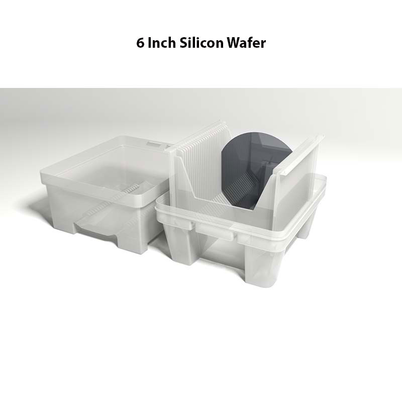
3) 6 inch (150mm) silicon wafers
Six-inch wafers are widely used for specialty analog, MEMS, sensors, and power devices. The 150mm platform can deliver strong die count improvements over 100mm without forcing a full leap to a 200mm toolset.
Why 150mm remains popular
- Balanced capex: Many mature lines already support 150mm tools and process recipes.
- Good die count: A clear step up from 4" for production-like runs.
- Long lifecycles: Ideal for automotive and industrial devices that run for years.
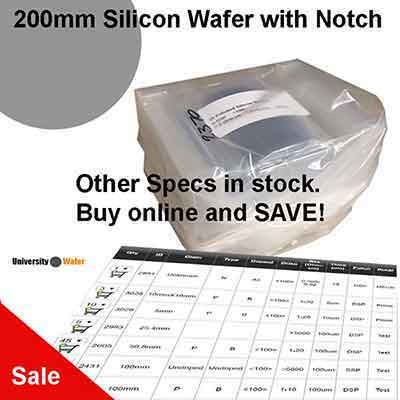
4) 8 inch (200mm) silicon wafers
Eight-inch wafers are the biggest “step change” for many specialty operations. You can often lower cost per die and increase throughput, especially if your fab has access to 200mm-compatible lithography, track systems, etch, deposition, and metrology tools.
Die count and throughput
The key benefit of 200mm is simple: more usable area per wafer. If you can keep yield stable, the cost per die generally improves because each run produces more devices. That is why many modernization efforts focus on 200mm lines for power and RF, where the economics can be very favorable.
5) Side-by-side comparison
| Attribute | 4" (100mm) | 6" (150mm) | 8" (200mm) |
|---|---|---|---|
| Best for | Lab R&D, prototypes, teaching | MEMS, analog, power, specialty lines | Higher throughput specialty, scaling production |
| Tool compatibility | Very high with legacy tools | High in mature specialty fabs | Requires 200mm-capable toolset |
| Capex | Low | Moderate | Higher (below 300mm) |
| Throughput | Low to medium | Medium | Medium to high |
6) A practical selection checklist
- What tools do you already have? Start with the largest diameter your lithography and handling support reliably.
- What is your volume target? Early R&D favors 4"; sustained specialty production often favors 6"; scale-up can favor 8".
- What does your device need? Prime surfaces for demanding layers, test/mechanical for fixtures, carriers, or non-critical studies.
- What electrical spec is required? Choose P-type, N-type, or undoped plus resistivity range based on your device design.
7) Grades and doping: what to match to your process
Diameter is only one part of wafer selection. Grade and doping frequently determine whether your wafer performs in-process and whether your final device meets spec.
- Prime grade: Best surface quality and tighter tolerances for device fabrication.
- Test grade: Cost-effective for development runs where minor defects are acceptable.
- Mechanical grade: Often used for monitors, carriers, or non-device applications.
Doping options such as boron (P-type) and arsenic/antimony (N-type) change conductivity and device behavior. If you are comparing runs, lock your orientation, resistivity, and dopant type before changing diameter so your data stays clean.
Conclusion
The best wafer size is the one that matches your equipment, your device requirements, and your scale timeline. Four-inch wafers are excellent for agile research and early prototypes. Six-inch wafers support many high-value specialty devices without forcing a full tool conversion. Eight-inch wafers can improve throughput and cost per die when your process and tool set are ready.
If you want, you can start with the size your tools support today and build a staged path that scales from 4" to 6" to 8" as demand and funding grow.