
InGaAs Wafers for Research and Device Development
Indium Gallium Arsenide (InGaAs) is a III-V compound semiconductor alloy commonly used in infrared detection, photonics, high-speed electronics, spectroscopy, optoelectronics, and advanced semiconductor research. Its direct bandgap and high electron mobility make InGaAs especially useful for devices that operate in near-infrared and high-frequency applications.
UniversityWafer supplies InGaAs wafers, InGaAs epitaxial layers, and InGaAs on InP structures for research, prototyping, and device development. Specifications may include custom compositions, doping levels, orientations, layer thicknesses, substrate types, and quantities.
For a broader overview of material properties and applications, visit our Indium Gallium Arsenide (InGaAs) resource page.
Get Your InGaAs Wafer Quote FAST! Or, Buy Online and start researching today!
What Are InGaAs Wafers Used For?
InGaAs wafers and epitaxial structures are used in applications where high carrier mobility and sensitivity to near-infrared wavelengths are important. Common research and device applications include:
- Near-infrared photodetectors and imaging sensors
- Optical communications and fiber-optic receivers
- High-speed and high-frequency transistors
- Integrated photonics and optoelectronic devices
- Spectroscopy and scientific instrumentation
- Thermophotovoltaic and photovoltaic research
InGaAs Photodetectors and Infrared Sensors
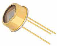
InGaAs is widely used in near-infrared photodetectors because its bandgap allows it to detect wavelengths that extend beyond the response range of conventional silicon photodiodes. InGaAs detector structures are used in optical communications, spectroscopy, imaging, sensing, and scientific instrumentation.
InGaAs for High-Speed Electronics
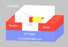
InGaAs is also studied for high-speed electronic devices because of its high electron mobility. InGaAs channels can be used in advanced transistor structures designed for high-frequency, low-power, and high-performance semiconductor applications.
InGaAs on InP and Other Substrates
InGaAs is commonly grown epitaxially on indium phosphide (InP). A composition near In0.53Ga0.47As is closely lattice matched to InP, which helps reduce strain and crystal defects in the epitaxial layer.
Growing InGaAs directly on silicon is more challenging because of lattice mismatch and differences in crystal properties. Researchers may use buffer layers, engineered heterostructures, or other integration techniques when combining InGaAs with silicon-based platforms.
UniversityWafer can help source InGaAs and InP substrates, epitaxial structures, and custom specifications for semiconductor research.
InGaAs Wafers and Epitaxial Structures
Indium Gallium Arsenide (InGaAs) is a III-V semiconductor alloy known for its high electron mobility and strong response in the near-infrared region. These properties make InGaAs useful for photodetectors, optical communications, spectroscopy, high-speed electronics, photonics, and semiconductor research.
UniversityWafer supplies InGaAs wafers and InGaAs epitaxial structures for research and device development, including InGaAs layers grown on indium phosphide (InP).

Why InGaAs Is Commonly Grown on InP
A composition near In0.53Ga0.47As is closely lattice matched to InP. This helps minimize strain and crystal defects when InGaAs is grown epitaxially on an InP substrate.
InGaAs-on-InP structures are widely studied for infrared photodetectors, photodiodes, optical receivers, integrated photonics, and other optoelectronic devices.
InGaAs Wafer Specifications
When selecting an InGaAs wafer or epitaxial structure, researchers may need to specify several material and device parameters, including:
- InGaAs alloy composition
- Substrate material, such as InP
- Wafer diameter
- Crystal orientation
- Substrate thickness
- Epitaxial layer thickness
- N-type, P-type, or undoped material
- Dopant type and carrier concentration
- Single-side or double-side polishing
- Layer structure and interface requirements
InGaAs for Infrared Detection
InGaAs is widely used for near-infrared detection because its band structure allows it to respond to wavelengths beyond the useful detection range of conventional silicon photodiodes.
InGaAs detector structures are commonly used in fiber-optic communications, spectroscopy, imaging, sensing systems, scientific instrumentation, and laser measurement.
InGaAs for High-Speed Electronics and Photonics
The high electron mobility of InGaAs also makes it useful for high-speed and high-frequency electronic devices. InGaAs can be incorporated into advanced transistor structures, photonic devices, optical receivers, and other III-V semiconductor systems.
Depending on the application, researchers may require custom epitaxial compositions, dopant concentrations, thicknesses, or multilayer structures.
Current InGaAs Inventory - Buy Online!
50.8 mm InGaAs Epi on InP
Substrate: 2-inch (50.8 mm) Indium Phosphide (InP), (100) orientation, approximately 350 µm thick, single-side polished.
N-Type Epitaxial Layer: Lattice-matched InGaAs:Si, (100) ±0.5°, approximately 1.0 µm thick (±20%), carrier concentration approximately 1 × 10¹⁷ to 1 × 1018 cm-3.
P-Type Epitaxial Layer: Lattice-matched InGaAs:Zn, (100) ±0.5°, approximately 1.0 µm thick (±20%), carrier concentration approximately 1 × 10¹⁷ to 1 × 1018 cm-3.
Wafers may be sealed individually in wafer containers.
50.8 mm InP / InGaAs / InP Epitaxial Wafers
Substrate: Indium Phosphide (InP), approximately 50.8 mm diameter and 380 ± 25 µm thick, N-type, (100) ±0.5°.
Surface: One-side polished with a matte-etched backside and SEMI-style flats.
Epitaxial Layer 1: InGaAs, approximately 100 nm, used as an etch-stop layer.
Epitaxial Layer 2: InP, approximately 50 nm, used as a bonding layer.
Need a Custom InGaAs Wafer Specification?
UniversityWafer can help researchers source InGaAs wafers, InGaAs-on-InP epitaxial structures, and custom III-V semiconductor materials based on composition, thickness, doping, orientation, layer design, and quantity.
Related InGaAs & III-V Semiconductor Resources
- Indium Gallium Arsenide (InGaAs) – Learn about InGaAs properties, bandgap, infrared response, and applications in photonics, detectors, and high-speed electronics.
- Indium Phosphide (InP) Wafers – Explore InP substrates commonly used for lattice-matched InGaAs epitaxial structures and optoelectronic devices.
- III-V Semiconductor Materials – Explore compound semiconductor materials used in photonics, electronics, infrared sensing, and advanced device research.
- Gallium Arsenide (GaAs) Wafers – Learn about GaAs substrates for high-frequency electronics, optoelectronics, photonics, and semiconductor research.
- Compound Semiconductors – Learn about III-V and other compound semiconductor materials used for electronic and optical devices.
- Semiconductor Bandgap – Understand how semiconductor bandgap influences optical absorption, emission, and electronic device performance.
- Integrated Photonics – Explore semiconductor substrates and materials used to develop integrated photonic and optoelectronic devices.
- Photodiodes – Learn how semiconductor materials such as InGaAs are used for optical and near-infrared detection.