
Indium Antimonide Wafers for Advanced Research
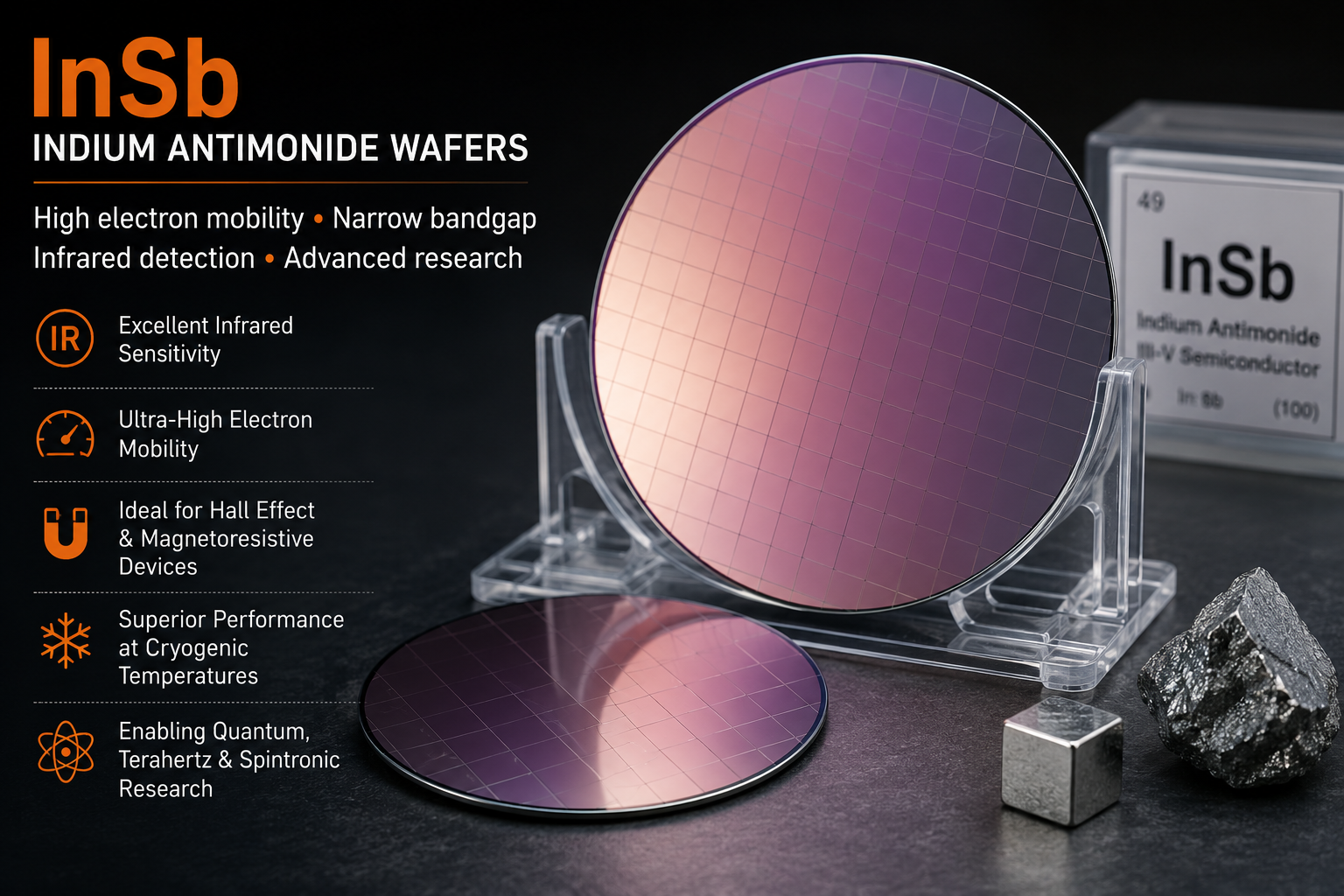
Indium Antimonide (InSb) wafers provide researchers with a specialized III-V semiconductor substrate for developing infrared, electronic, magnetic, and quantum devices. InSb has a narrow direct bandgap and exceptionally high electron mobility, making it valuable for experiments that require rapid carrier transport and strong sensitivity to infrared radiation.
Researchers commonly use InSb substrates to fabricate mid-wave infrared detectors, Hall effect sensors, magnetoresistive devices, high-speed transistors, and experimental quantum structures. The material is also studied for spintronics, two-dimensional electron gases, terahertz technologies, and low-power semiconductor devices.
How to Select an InSb Wafer
Selecting the appropriate InSb substrate depends on the device structure, fabrication process, and electrical performance required for your research. Important specifications may include:
- Crystal orientation: Common orientations include (100), (110), and (111).
- Conductivity type: Select undoped, n-type, or p-type material when available.
- Carrier concentration: Match the doping level to the intended electrical or detector application.
- Wafer diameter: Choose a substrate size compatible with your laboratory equipment.
- Wafer thickness: Consider handling strength, thermal behavior, and device-processing requirements.
- Surface finish: Single-side polished or double-side polished wafers may be required for lithography, epitaxy, or optical experiments.
InSb for Infrared Detector Research
The narrow bandgap of InSb makes it especially useful for infrared sensing and imaging. InSb substrates can support research involving cooled photodetectors, thermal imaging arrays, infrared spectroscopy, astronomy instrumentation, environmental monitoring, and other systems operating in the mid-wave infrared region.
For projects requiring a different infrared or compound-semiconductor platform, researchers may also compare InSb with Indium Arsenide wafers , Indium Phosphide wafers , or Gallium Arsenide wafers .
InSb Research Applications
- Mid-wave infrared photodetectors and imaging arrays
- Hall effect and magnetic-field sensors
- Magnetoresistive semiconductor devices
- High-speed and low-power transistor research
- Quantum wells and two-dimensional electron gases
- Spintronics and quantum-device development
- Terahertz emitters and detectors
- Infrared spectroscopy and optical characterization
Need a Custom InSb Wafer Specification?
UniversityWafer can help researchers locate InSb substrates based on orientation, diameter, thickness, conductivity type, carrier concentration, mobility, and surface finish. Send us the specifications required for your experiment, along with the quantity needed, and our team will help identify an appropriate substrate.
Get Your Indium Antimonide Wafer Quote FAST! Or Buy Online and Start Researching Today!
What Is an Indium Antimonide (InSb) Wafer?
An Indium Antimonide (InSb) wafer is a single-crystal III-V semiconductor substrate composed of indium (In) and antimony (Sb). InSb is well known for its exceptionally high electron mobility, narrow direct bandgap of approximately 0.17 eV at room temperature, and strong sensitivity to infrared wavelengths. These properties make InSb one of the preferred semiconductor materials for infrared imaging, Hall-effect sensors, magnetoresistive devices, high-speed electronics, and quantum research.
Compared to many conventional semiconductor materials, InSb enables faster electron transport and excellent performance at cryogenic temperatures. As a result, it is widely studied for advanced electronic devices, terahertz technologies, spintronics, and experimental quantum systems.
Key Properties of InSb
| Property | Typical Value |
|---|---|
| Crystal Structure | Zinc Blende (Cubic) |
| Bandgap | ~0.17 eV (300 K) |
| Electron Mobility | Up to 77,000 cm²/V·s |
| Lattice Constant | 6.479 Å |
| Density | 5.78 g/cm³ |
| Melting Point | 525°C |
| Common Orientations | (100), (110), (111) |
| Available Surface Finish | SSP or DSP |
Common Applications of InSb Wafers
Because of its unique electrical and optical characteristics, InSb is widely used in both commercial and university research laboratories. Typical applications include:
- Mid-wave infrared (MWIR) detectors
- Thermal imaging systems
- Infrared focal plane arrays
- Hall-effect magnetic sensors
- Magnetoresistance research
- Quantum computing and spintronics
- High-speed electronic devices
- Terahertz emitters and detectors
- Cryogenic semiconductor research
- Scientific spectroscopy instrumentation
Why Researchers Choose InSb
Researchers select InSb when maximum carrier mobility and infrared sensitivity are critical. Its narrow bandgap allows efficient detection of longer infrared wavelengths, while its outstanding electron mobility supports ultra-fast device operation. InSb is frequently chosen for experimental semiconductor devices, advanced sensor development, and fundamental materials research where high-speed carrier transport is essential.
Available InSb Wafer Specifications
UniversityWafer can source Indium Antimonide wafers in multiple diameters, crystal orientations, conductivity types, thicknesses, and polishing options. Depending on availability, researchers may request custom specifications for detector fabrication, epitaxial growth, MEMS, photonics, and semiconductor device development.